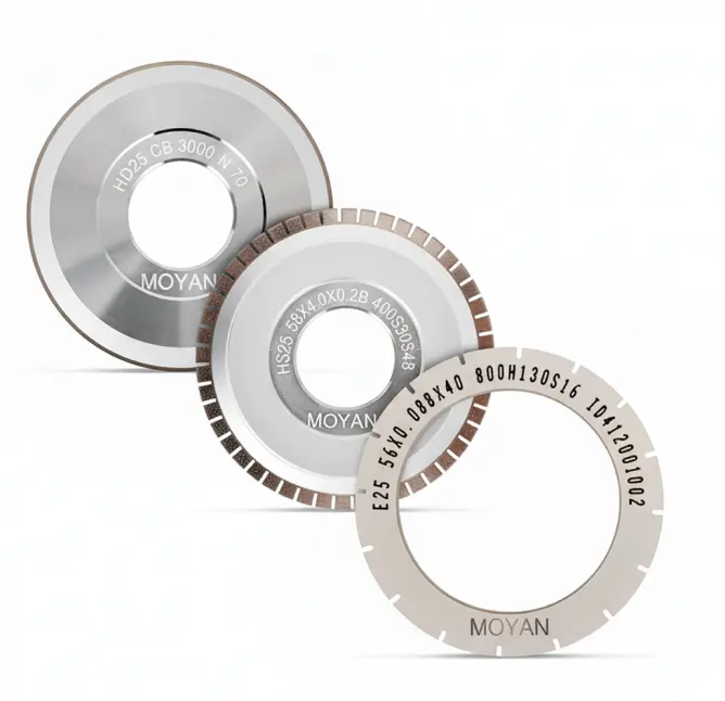
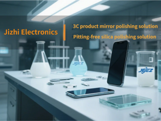
Our
Products
Precision dicing blades, waxless polishing pads, and CMP
slurries designed for stable and high-yield semiconductor
processes.

Our
Technological Advantages
Advanced manufacturing and strict quality control ensure
consistent performance in demanding applications.


Our
Solution
Application-focused solutions for dicing, polishing, and CMP
processes across different materials.
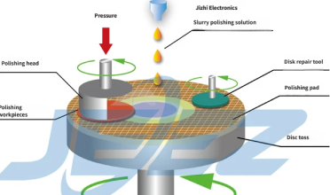
CMP (Chemical Mechanical Polishing) is currently the only technology used in modern industrial manufacturing for surface polishing of workpieces and global planarization of wafer surfaces in integrated circuit manufacturing. The CMP process achieves surface polishing through chemical and mechanical actions. It is widely applied in integrated circuit technology, wafer chip planarization, aerospace materials, the metal industry, and mirror polishing of materials in the optoelectronic industry. Schematic Diagram of Jizhi Electronics CMP Polishing Process Based on the type of material being polished, CMP can be divided into three main categories: (1) Substrates: Primarily silicon materials. (2) Metals: Including Al/Cu metal interconnect ...
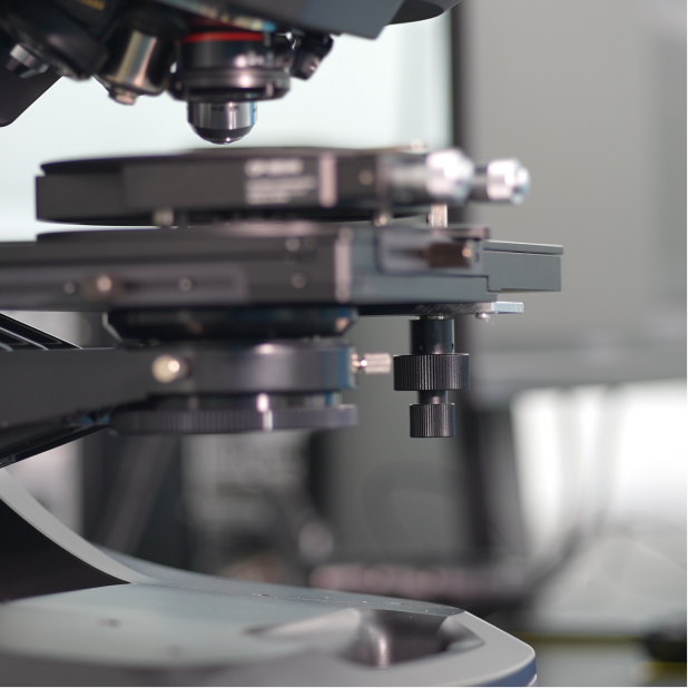
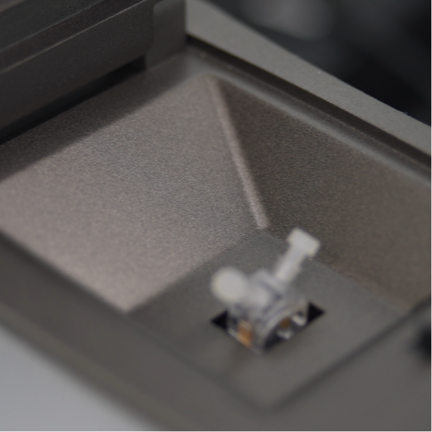
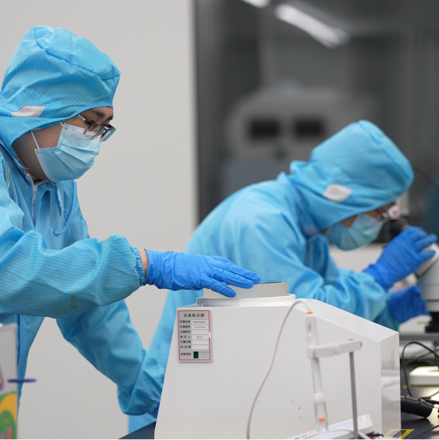
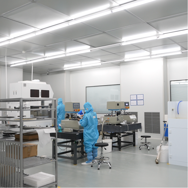
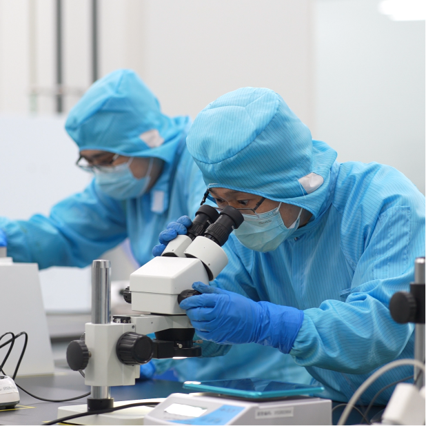
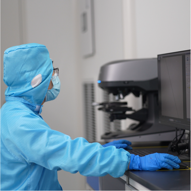
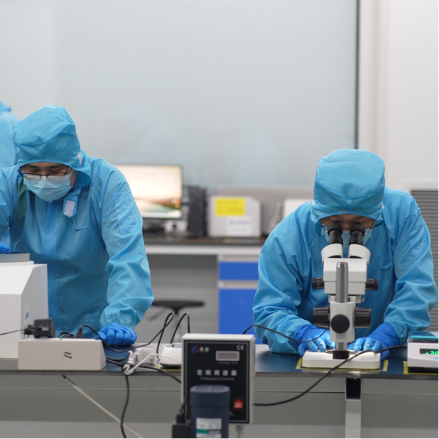
Our
Production equipment
Specialized production equipment supports high-precision
manufacturing and reliable product consistency.
Our
NEWS
Product updates, technical insights, and industry news from
semiconductor cutting and polishing.
Life assessment requires comprehensive monitoring of the following indicators:
| Monitoring Metric | Normal Range | Replacement Warning |
|---|---|---|
| Surface Porosity Change | Initial value ± 5% | > ± 15% |
| Elastic Recovery Rate | > 92% | < 85% |
| Friction Coefficient Stability | Fluctuation < ± 0.02 | Fluctuation > ± 0.05 |
| Slurry Consumption Rate | Baseline ± 10% | Increase > 25% |
Smart Monitoring Solution: We offer optional embedded sensor pads that transmit real-time pressure/temperature data to customer MES systems. Professional surface topography analysis is recommended after every 500 polishing cycles.
Three special requirements must be met:
-
Low-stress polishing: Elastic substrate modulus must match GaN’s brittle nature (fracture toughness < 2 MPa·m¹/²) to prevent micro-cracks
-
Resistance to strong alkaline environments: PTFE-modified polyurethane enables stable operation > 200 hours in KOH-based slurries with pH > 12
-
Enhanced thermal management: Thermal conductivity > 0.5 W/m·K for rapid dissipation of localized friction heat (GaN is temperature-sensitive)
Jizhi Electronics’ GaN-specific pad series has been validated in 6-inch wafer mass production, with warpage control < 50 µm.
Improvement can be quantified through three key metrics:
-
TTV Improvement: Proprietary porous elastic layer design controls wafer total thickness variation to < 0.3 µm (40% improvement over conventional pads)
-
Removal Rate Uniformity: Micro-channel technology improves within-wafer non-uniformity (WIWNU) to > 95%
-
Defect Control: Flexible fiber surface structure reduces scratch defect density to < 0.05 counts/cm²
We offer free process audit services to provide customers with benchmark comparison reports.