Silicon Wafer Surface Defects in CMP: Causes, Detection & Prevention
A comprehensive reference for engineers managing defect yield in silicon wafer CMP — classifying scratches, COPs, LPDs, haze, and edge roll-off; tracing each to its root cause; and presenting evidence-based prevention strategies.
Why Defect Control Is the #1 CMP Yield Challenge
A single scratch on a polished silicon wafer detected during laser-scanning surface inspection triggers immediate wafer rejection, writing off all upstream manufacturing cost — ingot growth, slicing, lapping, etching, and polishing — that may represent $200–500 per wafer. Defect control in silicon wafer CMP is therefore not a quality-assurance afterthought; it is the primary economic driver of the polishing operation.
This guide from Jizhi Electronic Technology Co., Ltd. (JEEZ) classifies the five major types of CMP defects encountered in silicon wafer polishing, traces each to its root cause, explains how they are detected, and presents the process engineering strategies that minimize them. For a broader context, see our Complete Guide to Silicon Wafer Polishing.
Defect Type 1 — Scratch Defects
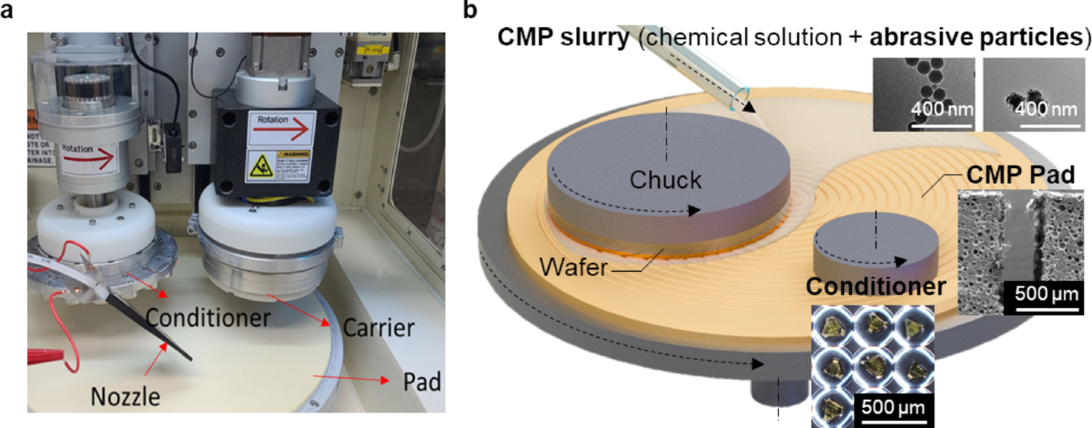
Scratches are the highest-severity defect class in silicon wafer CMP. They appear as linear or arc-shaped grooves on the wafer front surface, with widths ranging from ~0.05 μm (borderline detectable) to several micrometers and lengths from tens of micrometers to full-wafer arcs traversing most of the 300mm diameter. Scratches are detected during laser-scanning surface inspection (e.g., KLA Surfscan SP series) as elongated high-signal events with a specific shape signature that distinguishes them from round particles or pits.
Root Causes of Scratches
- Killer particles in slurry: Abrasive agglomerates >500 nm that lodge between the pad and the wafer surface and are dragged across the wafer by the rotating pad. These are the most common and most preventable scratch source. Agglomerates form when slurry pH drifts outside the stability window, when slurry sits stagnant in delivery lines (sedimentation followed by flow disruption), or when slurry exceeds its shelf life.
- Pad debris: Fragments of pad material shed during polishing or conditioning can act as abrasive bodies. This is more common after aggressive conditioning or when a new pad is improperly broken in.
- Environmental contamination: Particles from the cleanroom environment, from polishing tool internals (bearing wear, retaining ring fragments), or from inadequate tooling maintenance enter the slurry dispense path and appear at the wafer surface.
- Slurry cross-contamination: Residual rough-polish slurry (larger particles) carry-over into the finish-polish step, where their particle size is grossly mismatched to the soft pad and low-pressure conditions.
Prevention
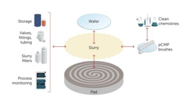
- Install 0.2–0.5 μm point-of-use filters on all slurry delivery lines
- Monitor slurry D99 and Dmax with single-particle optical sensing (SPOS/LFI) — not just DLS D50
- Implement slurry delivery line flush protocols after tool idle periods (>30 min)
- Perform a DI water or dilute acid quench rinse between rough and finish polish steps
- Execute a proper pad break-in protocol after each pad change
Defect Type 2 — Crystal-Originated Pits (COPs)
COPs (Crystal-Originated Pits) are octahedral vacancy-cluster voids present in the bulk Czochralski-grown silicon crystal before any polishing occurs. They form during crystal growth when the ingot cools through a critical temperature range: silicon vacancies condense into octahedral void clusters of 50–200 nm diameter. In standard (non-COP-free) CZ silicon, COPs occur at densities of 10²–10⁴ cm⁻³.
During alkaline CMP, the polishing process intersects the sub-surface void clusters and the interior of each void — which lacks a silicon crystal lattice on its exposed faces — etches faster than the surrounding perfect crystal. The result is a characteristic octahedral pit on the polished surface with a size of 0.1–0.3 μm, classified as a COP-related LPD on surface inspection.
Mitigating COP Manifestation in Polishing
- Use COP-free (or COP-reduced) silicon crystal from ingot growers who use controlled V/G growth conditions, nitrogen doping, or hydrogen annealing to suppress vacancy cluster formation
- Avoid over-aggressive alkaline chemistry in the finish polish (pH >11.2 at elevated temperature) which accelerates void interior etching and enlarges pits
- Hydrogen annealing of polished wafers (1150–1200°C in H₂ atmosphere) fills and annihilates near-surface COPs — a process option for zero-COP epi-ready wafer production
Defect Type 3 — Light Point Defects (LPDs) and Particles
Light point defects are the primary pass/fail metric for polished silicon wafer quality. On a KLA Surfscan SP3 or SP5 system, the wafer is illuminated with a focused laser beam in dark-field mode; any surface feature that scatters light above the detection threshold (typically 35 nm or 60 nm calibrated sphere diameter equivalent) registers as an LPD event. LPDs include particles, pits, mounds, and surface anomalies of all physical origins.
In the context of CMP process control, the key LPD sources are:
- Residual slurry abrasive: Colloidal silica particles that adhere to the polished surface and are not removed by post-CMP cleaning. Electrostatic adhesion between the slightly positive silicon surface and negatively charged silica particles can be surprisingly strong, especially if the pH drops during the rinse sequence.
- Re-deposited silicon species: Dissolved SiO₂·nH₂O from the polishing reaction can re-precipitate as amorphous silica micro-deposits during rinsing, particularly if the rinse water temperature or pH is not well-controlled.
- Pad debris and atmospheric particles: Small fragments from pad conditioning or ambient contamination that land on the wafer surface during or after polishing.
Achieving LPD counts below 30 at 35 nm on 300mm wafers requires both excellent slurry quality and a highly effective post-CMP cleaning sequence. For cleaning protocols, see: Post-CMP Cleaning for Silicon Wafers: Methods and Best Practices.
Defect Type 4 — Surface Haze
Haze is not a discrete defect but a spatially distributed surface characteristic: the intensity of diffuse scattered light from micro-roughness across the wafer surface, measured in parts per million (ppm) of incident light intensity. Haze arises from surface features at spatial wavelengths between ~1 and ~10 μm — too small to resolve as individual LPDs but collectively measurable as a background signal on the surface inspector.
Haze has two distinct origins in CMP:
- Roughness haze: Micro-roughness at the 1–10 μm spatial frequency range, typically produced by over-polishing (where isotropic chemical etching roughens the crystal surface along crystallographic directions), by mechanical abrasion from an overly stiff pad or overly large slurry particles, or by pad-to-wafer contact non-uniformity that creates azimuthal roughness patterns.
- Contamination haze: Thin chemical contamination films — residual slurry organic additives, silicic acid re-deposits, or oxidation films — that create a spatially uniform increase in scattered light intensity rather than discrete LPD events.
Haze is controlled by optimizing the SSP finish polish parameters (slurry pH, particle size, pad hardness, pressure, and polish time) and by ensuring effective post-CMP cleaning removes all chemical residues before inspection. For detailed guidance on achieving sub-0.03 ppm haze levels, see: How to Achieve Sub-nm Surface Roughness in Silicon Wafer CMP.
Defect Type 5 — Edge Roll-off and Edge Exclusion
The wafer edge zone — typically defined as the outermost 2–5 mm of the wafer radius — is the most geometrically challenging region in CMP. The polishing pad extends beyond the wafer edge during processing; as it does so, the contact pressure distribution at the wafer periphery diverges from the contact mechanics in the central area. Depending on retaining ring load, pad stiffness, and slurry film thickness, the result is either edge-fast (roll-down) or edge-slow (roll-up) removal — both are referred to as “edge roll-off” and both produce SFQR failures at the outermost exposure sites.
Edge roll-off translates directly to yield loss: die sites in the edge exclusion zone cannot meet overlay specifications and are scrapped. Minimizing the edge exclusion zone from the standard 2 mm toward 1 mm is a significant yield-improvement opportunity at 300mm.
Control strategies include: retaining ring material and load optimization, edge profile (chamfer geometry) standardization, and carrier head edge zone pressure control in multi-zone membrane systems. For detailed 300mm edge management strategies, see: 300mm Silicon Wafer Polishing: Challenges and Uniformity Control.
Defect Detection and Metrology
Three principal metrology techniques characterize defect levels on polished silicon wafers:
- Laser-scanning surface inspection (Surfscan SP3/SP5, Candela CS920): Scans the entire wafer at high speed in dark-field illumination. Reports LPD count at specified size thresholds, haze level (ppm), and defect location maps. Essential for go/no-go quality control on every wafer.
- Atomic force microscopy (AFM): Provides true topographic maps at nanometer-scale resolution over 1×1 μm to 10×10 μm scan areas. Used to characterize roughness (Ra, Rq), identify scratch morphology, and confirm the nature of LPD events. Too slow for 100% production inspection; used for process development and failure analysis.
- Transmission electron microscopy (TEM) / cross-sectional SEM: Reveals sub-surface crystal damage, COP morphology, and the depth profile of scratch damage. Destructive technique used in root-cause analysis of defect events, not routine inspection.
Frequently Asked Questions
Reduce CMP Defects with JEEZ High-Purity Slurries
JEEZ CMP slurries are engineered with tightly controlled D99 particle size distributions and industry-leading colloidal stability to minimize killer particles and deliver consistent LPD performance. Request a product data sheet or defect benchmarking evaluation.
Contact JEEZ Technical Team