Analysis of Key Polishing and Lapping Processes for InP (Indium Phosphide) Substrates
Indium Phosphide (InP), as a core material of the third-generation semiconductor, holds an irreplaceable position in high-end fields such as optical communications, millimeter-wave radar, and quantum communications due to its excellent electron mobility, wide bandgap, and superior optoelectronic properties. The surface quality of InP substrates directly determines the precision and reliability of subsequent epitaxial growth and device fabrication, with polishing and lapping processes being the critical steps in controlling this core metric. Drawing on years of practical experience in semiconductor material processing, Gizhi Electronics provides a systematic analysis of the key polishing and lapping processes for InP substrates, along with related technologies and consumables (InP polishing slurry/polishing pads) for chemical mechanical polishing (CMP).
I. Lapping Process: Laying the Foundation for High Precision
The primary goal of the lapping process is to rapidly remove the cutting-damaged layer from the substrate surface, correct geometric shape deviations, and provide a flat, uniform surface base for subsequent polishing. Precise control of process parameters directly impacts lapping efficiency and surface flatness. Through extensive process validation, Gizhi Electronics has developed a mature lapping process system.
1. Core Equipment Selection
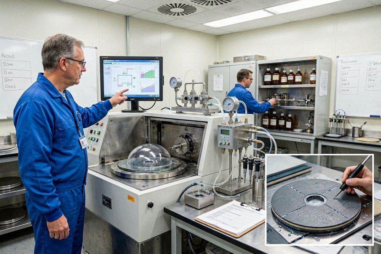
Double-sided planetary lapping machines / Chemical Mechanical Polishing (CMP) equipment are commonly used in industrial production. This equipment drives the InP substrates placed in carriers to perform compound motion through the counter-rotating planetary movement of the upper and lower plates, ensuring uniform force distribution and sufficient lapping across all areas of the wafer and effectively preventing edge warping issues common in single-sided belt lapping. The spindle accuracy and parallelism calibration of the lapping plates are prerequisites for ensuring lapping quality. Gizhi Electronics implements a regular calibration system for equipment to maintain operational accuracy within ±0.001 mm.
2. Control of Key Process Parameters
The matching of lapping parameters is key to achieving “efficient damage removal + low residual damage.” Considering InP’s high brittleness and susceptibility to cracking, Gizhi Electronics has optimized the following key parameter ranges:
① Lapping Pressure: Optimal range: 150–180 N. Insufficient pressure leads to low lapping efficiency and incomplete removal of the cutting-damaged layer, while excessive pressure can cause defects like crystal plane cracks and surface edge chipping. For thin substrates (thickness < 100 µm), the pressure should be further reduced to 120–150 N.
② Lapping Plate Speed: Lower plate speed is controlled at 4–8 RPM, with an upper-to-lower plate speed ratio of 1:1.2. Lower speeds reduce frictional heat between the wafer and the lapping plate, preventing surface oxidation of InP due to high temperatures. The speed ratio ensures uniform lapping trajectories and reduces surface waviness.
③ Abrasive Particle Size: Alumina (Al₂O₃) abrasive powder with a D50% of 4–12 µm is preferred. Particles that are too large can cause deep surface scratches, while particles that are too small significantly reduce the removal rate. Gizhi Electronics uses graded and screened abrasive powder to ensure particle size distribution deviation ≤10%.
3. Lapping Slurry Formulation and Supply
The lapping slurry consists of water, alumina abrasive, suspending agents, and a small amount of pH adjuster. The Al₂O₃ abrasive is selected as high-purity particles (purity ≥99.9%) of 400–600 mesh to minimize impurity contamination. Suspending agents such as Polyvinyl Alcohol (PVA) or Carboxymethyl Cellulose (CMC) are used to ensure uniform dispersion of the abrasive and prevent uneven lapping due to settling. A constant-pressure liquid delivery system supplies the slurry at a stable flow rate of 500–800 mL/min, ensuring the lapping area remains continuously moistened and promptly removes lapping debris and heat.
4. Pre-Etching Auxiliary Process
For high-hardness InP substrates, Gizhi Electronics innovatively employs a “chemical pre-etching + mechanical lapping” composite process. The substrate surface is mildly etched with a mixed solution of hydrobromic acid, phosphoric acid, hydrochloric acid, and acetic acid (volume ratio 3:2:1:1), forming a porous “trabecular” structure. This structure reduces the Mohs hardness by over 30% compared to the original InP, significantly enhancing lapping efficiency and effectively preventing scratch propagation during lapping. Pre-etching time is strictly controlled to 30–60 seconds, followed immediately by rinsing with pure water to avoid residual acid causing grain boundary corrosion.
II. Polishing Process: Achieving a Mirror-Like Surface
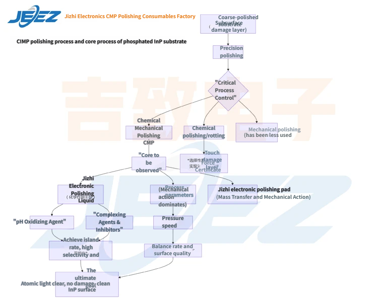
The polishing process is the critical step for eliminating residual lapping damage and achieving an atomically flat surface. Its core mechanism involves the synergistic action of “chemical corrosion + mechanical removal”: the oxidizer in the polishing slurry reacts chemically with the InP surface to form soluble phosphate compounds, which are then mechanically removed by the polishing pad and silica (SiO₂) colloidal particles through friction. This cycle repeats to refine the surface. Gizhi Electronics adopts a three-stage polishing process—rough polishing, medium polishing, and fine polishing—to progressively optimize surface quality.
1. Staged Process: Three-Stage Polishing
| Polishing Stage | Core Objective | Polishing Pad Selection | Polishing Slurry Configuration | Process Parameters |
|---|---|---|---|---|
| Rough Polishing | Quickly eliminate lapping scratches, initiate mirror finishing | Polyurethane/Hard Polishing Pad (Shore D Hardness ~50) | SiO₂ Colloid (100-150 nm) + Perchlorate Oxidizer (Effective Chlorine 8-10%), pH=10-11 | Pressure: 80-100 N, Speed: 10-15 RPM, Time: 15-20 min |
| Medium Polishing | Correct local flatness, reduce waviness | Polyurethane/Non-woven/Composite Pad (Shore D Hardness ~40) | SiO₂ Colloid (50-80 nm) + Hydrogen Peroxide (3-5%), pH=9-10 | Pressure: 50-70 N, Speed: 8-12 RPM, Time: 10-15 min |
| Fine Polishing | Eliminate micro-defects, achieve atomic-level flatness | Suba/Damping Cloth Fine Polishing Pad (Shore D Hardness ~30) | SiO₂ Colloid (20-40 nm) + Hydrogen Peroxide (1-2%), pH=8-9 | Pressure: 30-50 N, Speed: 5-8 RPM, Time: 20-25 min |
2. Critical Matching of CMP Slurry and Pad
InP’s high chemical stability necessitates the use of alkaline silica sol-based polishing slurries to enhance chemical corrosion. Oxidizer selection is particularly crucial: perchlorates, with their good solubility and oxidation potential, rapidly form a reaction layer during rough polishing, while hydrogen peroxide in the fine polishing stage allows controlled oxidation rates to prevent over-corrosion. Polishing pad selection must balance “removal rate” and “surface damage”: harder grooved pads improve efficiency during rough polishing, while softer suede-type pads minimize mechanical damage during fine polishing. Through customized pad surface textures, Gizhi Electronics achieves an optimal balance between removal rate and surface quality at each stage.
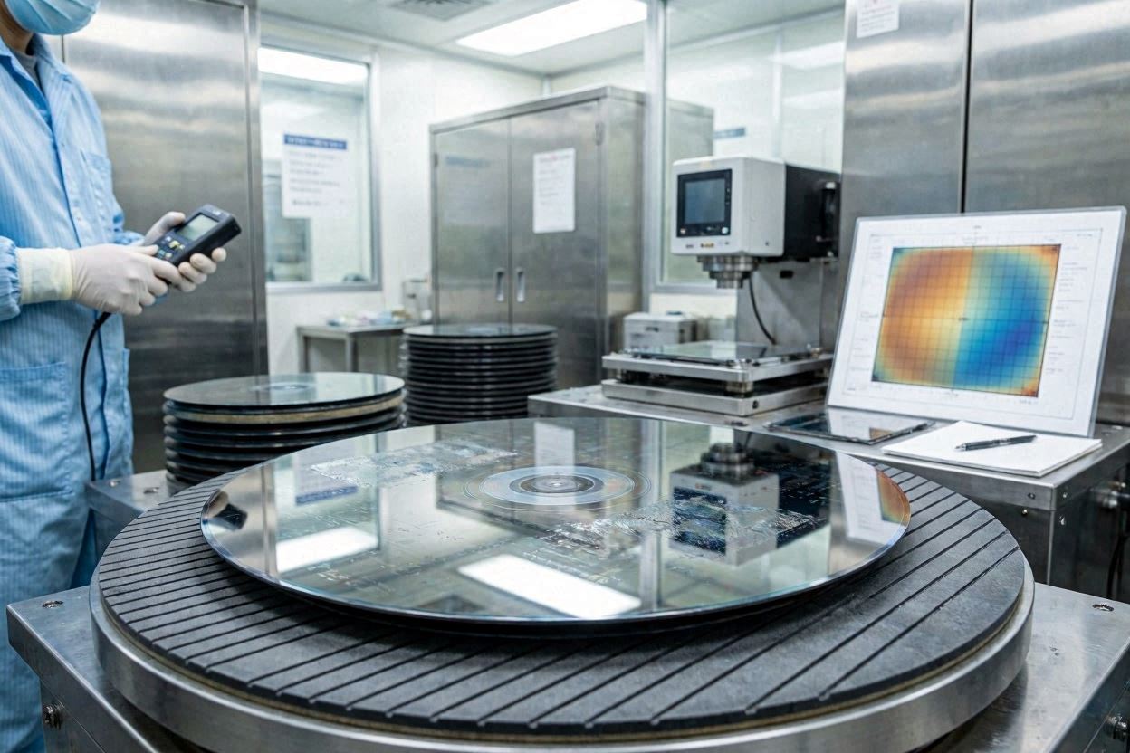
3. Polishing Environment and Post-Processing Control
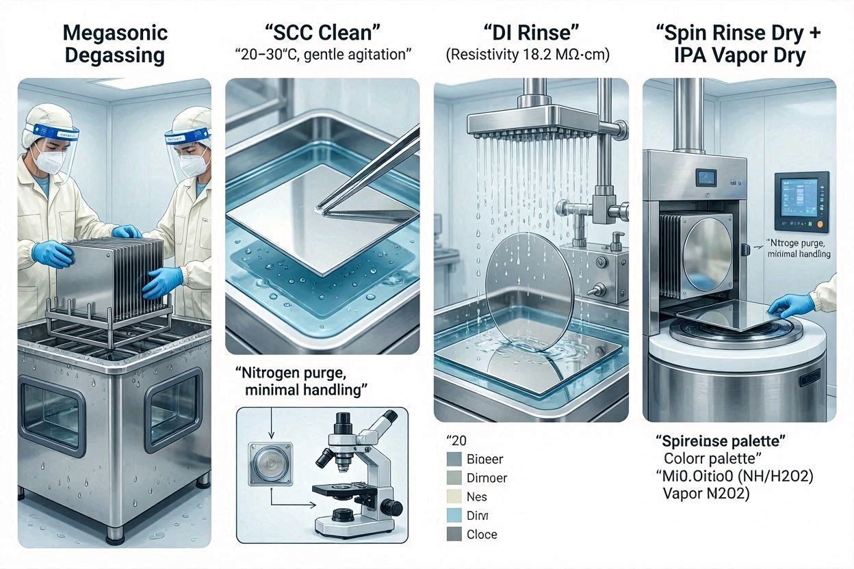
Polishing must be conducted in a Class 1000 cleanroom to prevent secondary contamination from airborne particulate impurities. After polishing, a three-stage cleaning process—”Ultrasonic Cleaning + Megasonic Cleaning + Spin Drying”—is immediately employed: first, ultrasonic cleaning with a neutral detergent at 50°C for 10 minutes to remove residual slurry; followed by megasonic cleaning (1 MHz frequency) to remove adhered micro-particles; and finally, spin drying at 1000 RPM for 5 minutes to ensure a water-mark-free surface.