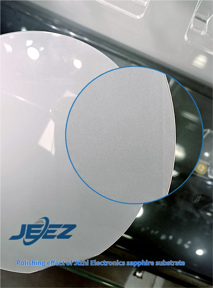
The purpose of polishing sapphire wafers is to reduce the final thickness of the substrate to the desired target value, achieving a TTV (Total Thickness Variation) of better than ±2 μm and a surface roughness of less than 2 nm. These operational requirements demand machinery and processes with high precision, efficiency, and stability. Using Gizhil Electronic’s sapphire polishing slurry and polishing pads for CMP (Chemical Mechanical Polishing) grinding and polishing enables the realization of this process.

By employing CMP polishing techniques, sapphire workpieces can achieve the desired surface roughness. Each polished sapphire wafer undergoes uniform material removal during processing, ensuring consistent surface finish. By adjusting the pressure load, a material removal rate (MRR) of 1–2 μm per hour can be achieved.
Sapphire wafer polishing is divided into A-plane polishing and C-plane polishing. From the perspective of sapphire’s crystal plane properties, the A-plane has higher hardness than the C-plane. Notably, smartphone screens, which belong to the A-plane sapphire crystal orientation, present the highest polishing difficulty. A-plane sapphire polishing generally consists of three stages: grinding, copper polishing, and fine polishing. The grinding stage serves to reduce the depth of surface step-like scratches caused during the cutting process of raw sapphire wafers. More importantly, it ensures that the thickness of batch-processed raw sapphire wafers is as consistent as possible.