logo

About semiconductor

This author has not yet filled in any details.
So far semiconductor has created 90 blog entries.

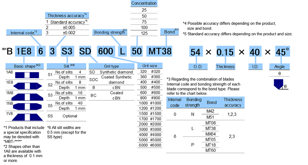
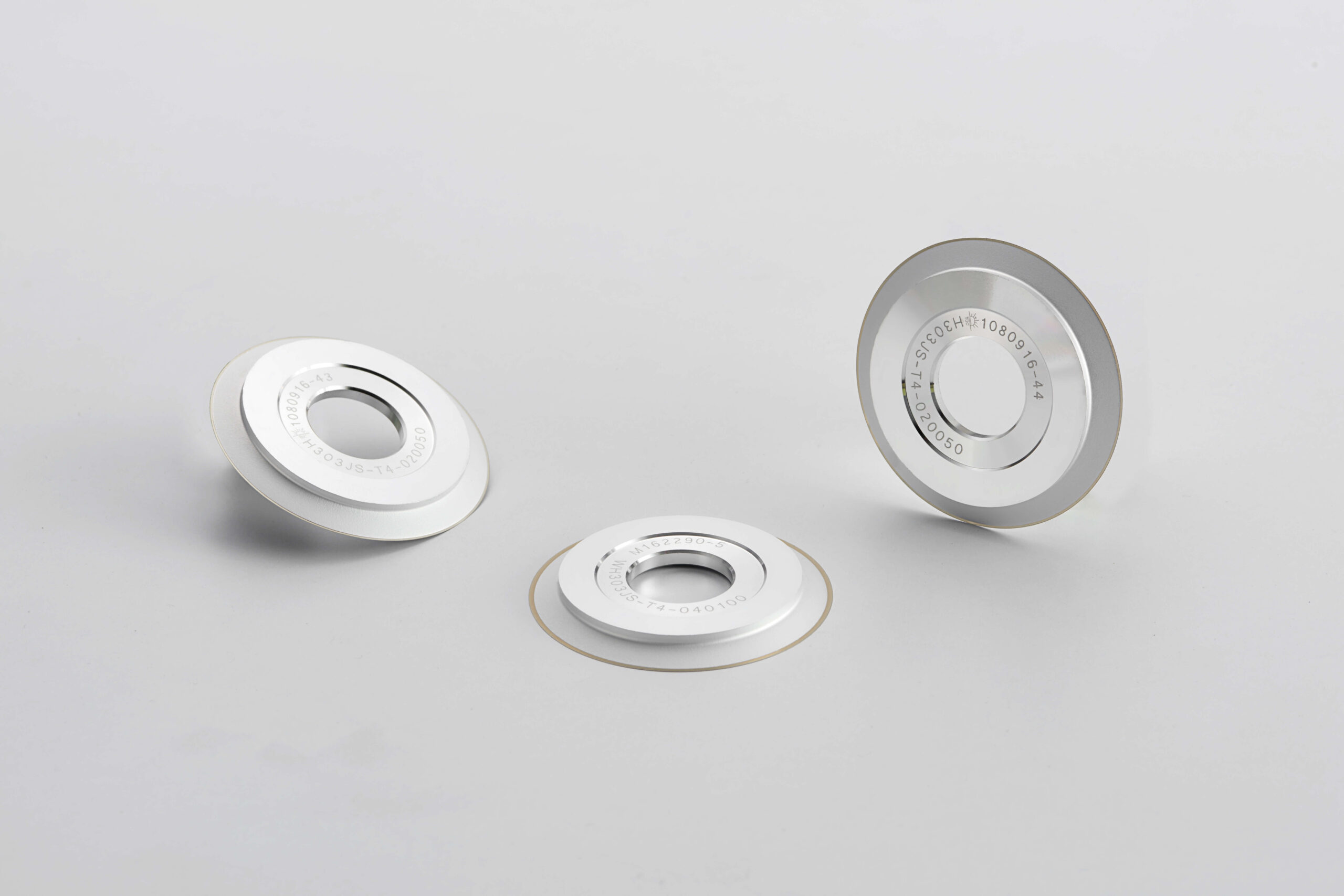
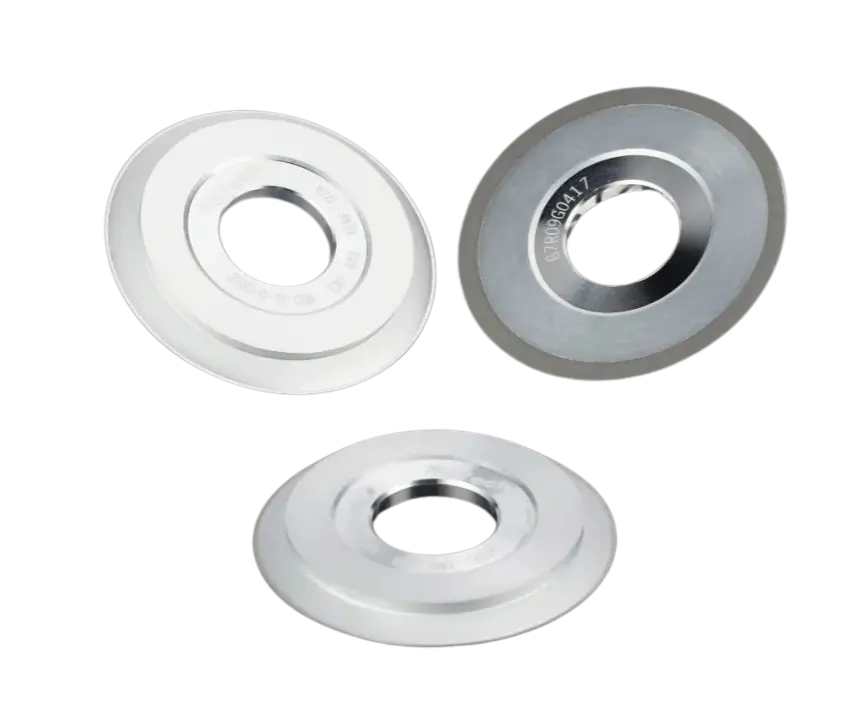
Dicing Blade Specifications Guide OD Thickness Grit Size and Exposure

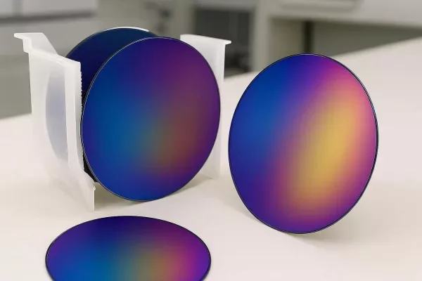
← Back to: Diamond Dicing Blades: The Complete Guide A dicing blade datasheet typically lists eight or more parameters, and choosing incorrectly on any one of them can result in ...

By |2026-03-16T09:43:44+08:002026年3月16日|Blog, Industry|0 Comments

Contamination Control in Polishing Templates: Clean Room Assembly & Particle Prevention

Contamination Control A single glass fiber fragment from a degraded polishing template carrier plate can scratch dozens of wafers before it is identified. Contamination control starts at template manufacturing — ...

By |2026-03-13T09:54:01+08:002026年3月13日|Blog, Industry|0 Comments

How to Extend Polishing Template Lifespan: Best Practices for Semiconductor Fabs

Fab Operations Best Practices Polishing templates are precision consumables — not commodity items to be used and discarded without discipline. The fabs that achieve the longest service life per template ...

By |2026-03-16T08:57:28+08:002026年3月13日|Blog, Industry|0 Comments

Why Is Your Wafer Edge Profile Poor? 5 Template-Related Causes & Solutions

Troubleshooting Guide Before adjusting your process recipe, check the template. Five specific template conditions account for the majority of edge profile excursions in production — and each one has a ...

By |2026-03-13T09:53:52+08:002026年3月13日|Blog, Industry|0 Comments

Polishing Templates for Glass Wafers & Ceramic Substrates: Key Considerations

Glass & Ceramic Substrates Glass and ceramic substrates span the widest thickness range, the most varied chemistries, and the most diverse geometries of any substrate category. Getting the polishing template ...

By |2026-03-13T09:53:47+08:002026年3月13日|Blog, Industry|0 Comments

Polishing Templates for Compound Semiconductor Wafers: GaAs, InP & Sapphire

Compound Semiconductor Substrates III-V compound semiconductors and sapphire demand polishing templates that silicon engineers rarely encounter: softer pads to protect fracture-prone crystals, chemically resistant carrier plates for bromine and acid ...

By |2026-03-13T09:53:43+08:002026年3月13日|Blog, Industry|0 Comments

SiC Wafer Polishing Templates: Chemically Resistant Solutions for Silicon Carbide Processing

SiC Substrate Engineering Silicon carbide is the hardest common semiconductor substrate and demands the most chemically aggressive CMP slurries. Standard polishing templates fail within weeks. This guide covers what SiC ...

By |2026-03-13T09:53:38+08:002026年3月13日|Blog, Industry|0 Comments
Go to Top