logo

About semiconductor

This author has not yet filled in any details.
So far semiconductor has created 206 blog entries.

Chemical Mechanical Planarization (CMP) Equipment: The Complete Guide

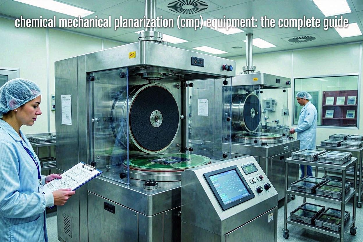
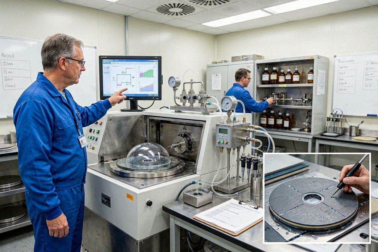
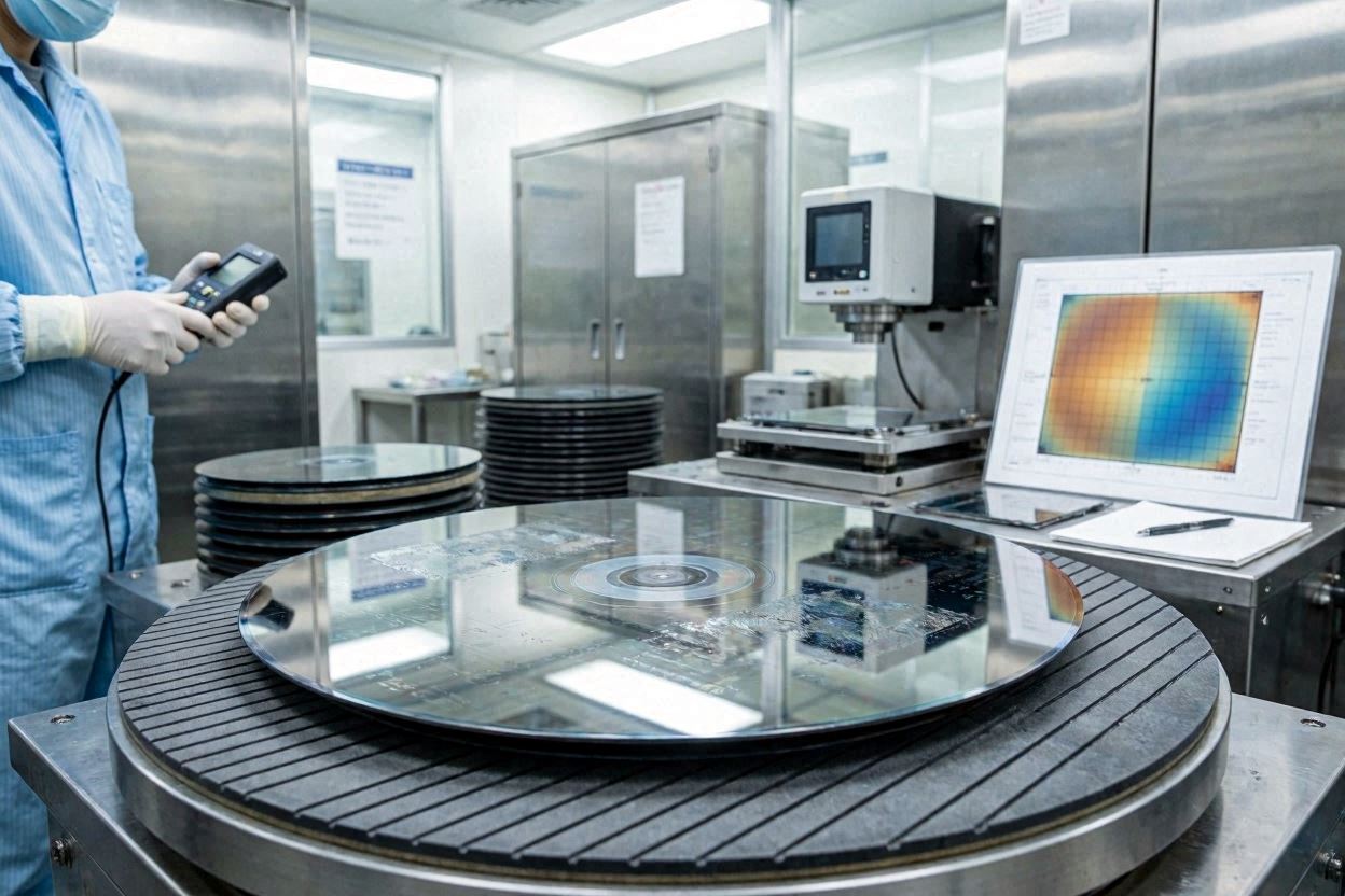
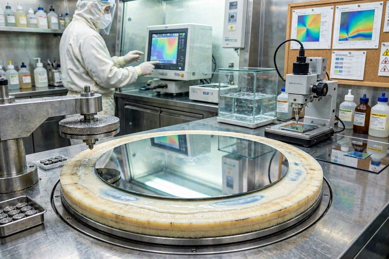
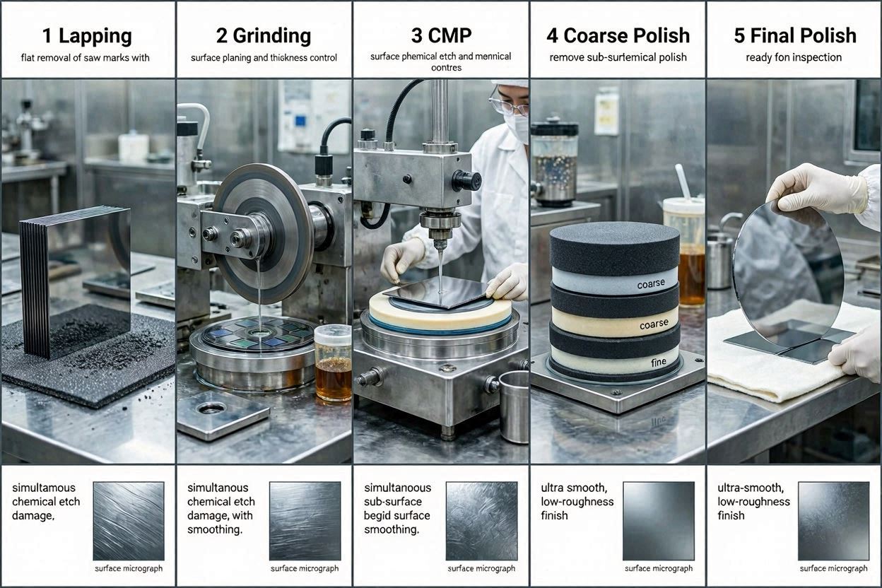
Chemical mechanical planarization (CMP) equipment sits at the heart of every modern wafer fab. Without it, the multilayer stacks of metal, dielectric, and barrier films that make up today's logic, ...

By |2026-06-15T16:02:36+08:002026年6月15日|Blog, Industry|Comments Off on Chemical Mechanical Planarization (CMP) Equipment: The Complete Guide

CMP Cost Optimization: How to Reduce Slurry Consumption and Improve Yield

← Back to: The Complete Guide to Silicon Wafer Polishing JEEZ Semiconductor Materials  ·  Technical Guide  ·  Updated June 2026 A systematic guide to reducing silicon wafer CMP operating costs ...

By |2026-06-09T15:54:04+08:002026年6月9日|Blog, Industry|Comments Off on CMP Cost Optimization: How to Reduce Slurry Consumption and Improve Yield

Post-CMP Cleaning for Silicon Wafers: Methods and Best Practices

← Back to: The Complete Guide to Silicon Wafer Polishing JEEZ Semiconductor Materials  ·  Technical Guide  ·  Updated June 2026 A complete technical guide to post-CMP cleaning — covering contamination ...

By |2026-06-09T15:53:59+08:002026年6月9日|Blog, Industry|Comments Off on Post-CMP Cleaning for Silicon Wafers: Methods and Best Practices

300mm Silicon Wafer Polishing: Challenges and Uniformity Control

← Back to: The Complete Guide to Silicon Wafer Polishing JEEZ Semiconductor Materials  ·  Technical Guide  ·  Updated June 2026 A deep technical guide to the unique challenges of polishing ...

By |2026-06-09T15:53:54+08:002026年6月9日|Blog, Industry|Comments Off on 300mm Silicon Wafer Polishing: Challenges and Uniformity Control

How to Achieve Sub-nm Surface Roughness in Silicon Wafer CMP

← Back to: The Complete Guide to Silicon Wafer Polishing JEEZ Semiconductor Materials  ·  Technical Guide  ·  Updated June 2026 A process engineering guide to reaching Ra below 0.1 nm ...

By |2026-06-09T15:53:49+08:002026年6月9日|Blog, Industry|Comments Off on How to Achieve Sub-nm Surface Roughness in Silicon Wafer CMP

Colloidal Silica vs. Alumina Slurry for Silicon Wafer Polishing

← Back to: The Complete Guide to Silicon Wafer Polishing JEEZ Semiconductor Materials  ·  Technical Guide  ·  Updated June 2026 A detailed technical comparison of the two principal abrasive chemistries ...

By |2026-06-09T15:53:45+08:002026年6月9日|Blog, Industry|Comments Off on Colloidal Silica vs. Alumina Slurry for Silicon Wafer Polishing

Silicon Wafer Surface Defects in CMP: Causes, Detection & Prevention

← Back to: The Complete Guide to Silicon Wafer Polishing JEEZ Semiconductor Materials  ·  Technical Guide  ·  Updated June 2026 A comprehensive reference for engineers managing defect yield in silicon ...

By |2026-06-09T15:53:40+08:002026年6月9日|Blog, Industry|Comments Off on Silicon Wafer Surface Defects in CMP: Causes, Detection & Prevention

Single-Side vs. Double-Side Polishing: Which Is Right for Your Wafer?

← Back to: The Complete Guide to Silicon Wafer Polishing JEEZ Semiconductor Materials  ·  Technical Guide  ·  Updated June 2026 A complete technical comparison of SSP and DSP polishing architectures ...

By |2026-06-09T15:53:35+08:002026年6月9日|Blog, Industry|Comments Off on Single-Side vs. Double-Side Polishing: Which Is Right for Your Wafer?

Silicon Wafer Polishing Process: Step-by-Step from Lapping to Final Polish

← Back to: The Complete Guide to Silicon Wafer Polishing JEEZ Semiconductor Materials  ·  Technical Guide  ·  Updated June 2026 A detailed technical walkthrough of every stage in the silicon ...

By |2026-06-09T15:53:30+08:002026年6月9日|Blog, Industry|Comments Off on Silicon Wafer Polishing Process: Step-by-Step from Lapping to Final Polish

CMP Slurry for Silicon Wafer: Types, Selection & Best Practices

← Back to: The Complete Guide to Silicon Wafer Polishing JEEZ Semiconductor Materials  ·  Technical Guide  ·  Updated June 2026 A complete engineer's guide to colloidal silica, fumed silica, and ...

By |2026-06-09T15:53:24+08:002026年6月9日|Blog, Industry|Comments Off on CMP Slurry for Silicon Wafer: Types, Selection & Best Practices
Go to Top