
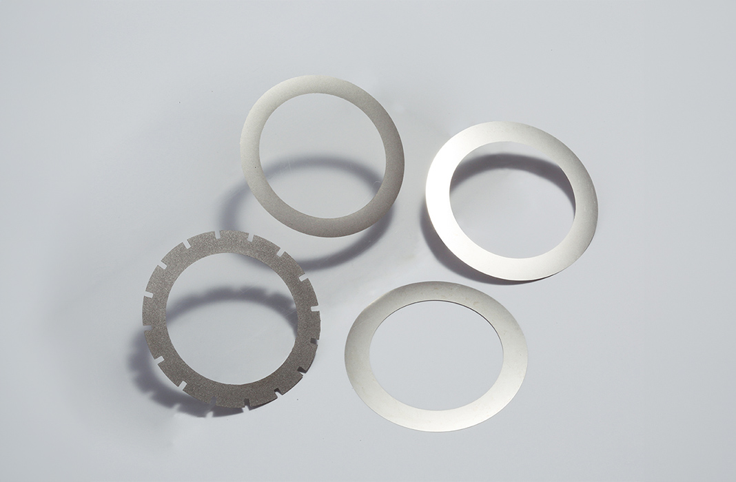
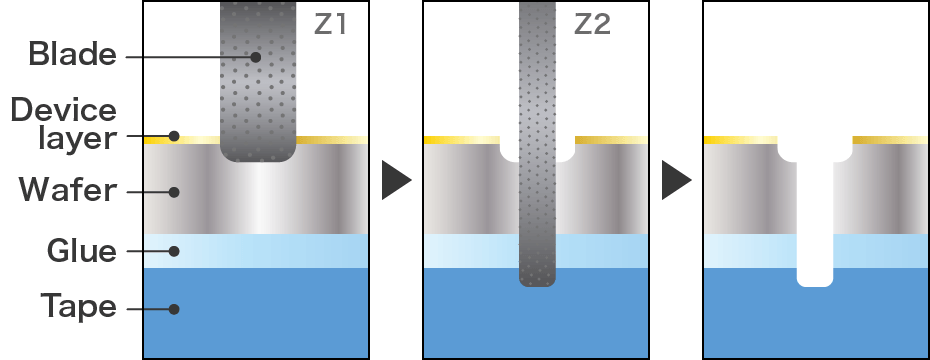
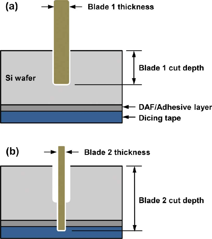
Dicing Saw Blade Width in Semiconductor Dicing
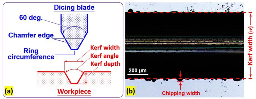
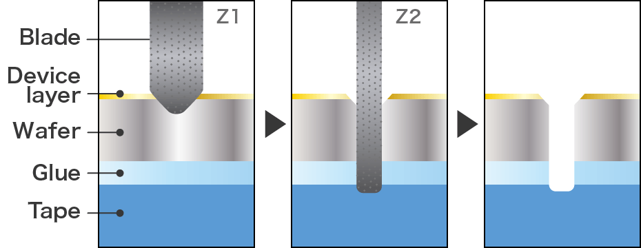
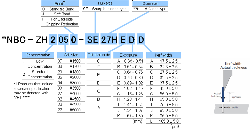
Dicing saw blade width is a critical parameter that directly determines kerf control, cutting precision, and blade path stability during wafer dicing. Although blade width is often discussed together with ...


