Blade Dicing Process for Semiconductor Wafers
The blade dicing process is the most widely adopted wafer singulation method in semiconductor manufacturing. Despite the emergence of alternative technologies such as laser dicing and stealth dicing, blade dicing remains the primary solution for high-volume production due to its flexibility, process controllability, and compatibility with a broad range of wafer materials. From a process engineering perspective, blade dicing is not a single cutting action, but a tightly controlled sequence of mechanical, thermal, and material-removal events.
This page provides a process-oriented explanation of blade dicing for semiconductor wafers. It focuses on how the process is executed step by step, which parameters must be controlled at each stage, and how blade dicing compares with other singulation methods from an engineering standpoint. The content is intended to support practical process development and optimization rather than theoretical discussion.
This cluster page complements the main pillar Wafer Dicing Blades for Semiconductor Applications and builds upon the material and cutting principles described in Dicing Blade Technology.
What Is the Blade Dicing Process?
Blade dicing is a mechanical wafer singulation process in which a rotating diamond dicing blade cuts through a semiconductor wafer along predefined scribe lines. The wafer is mounted on adhesive dicing tape, supported by a vacuum chuck, and indexed under a high-speed spindle. Material removal occurs through abrasive cutting and controlled brittle fracture at the blade–wafer interface.
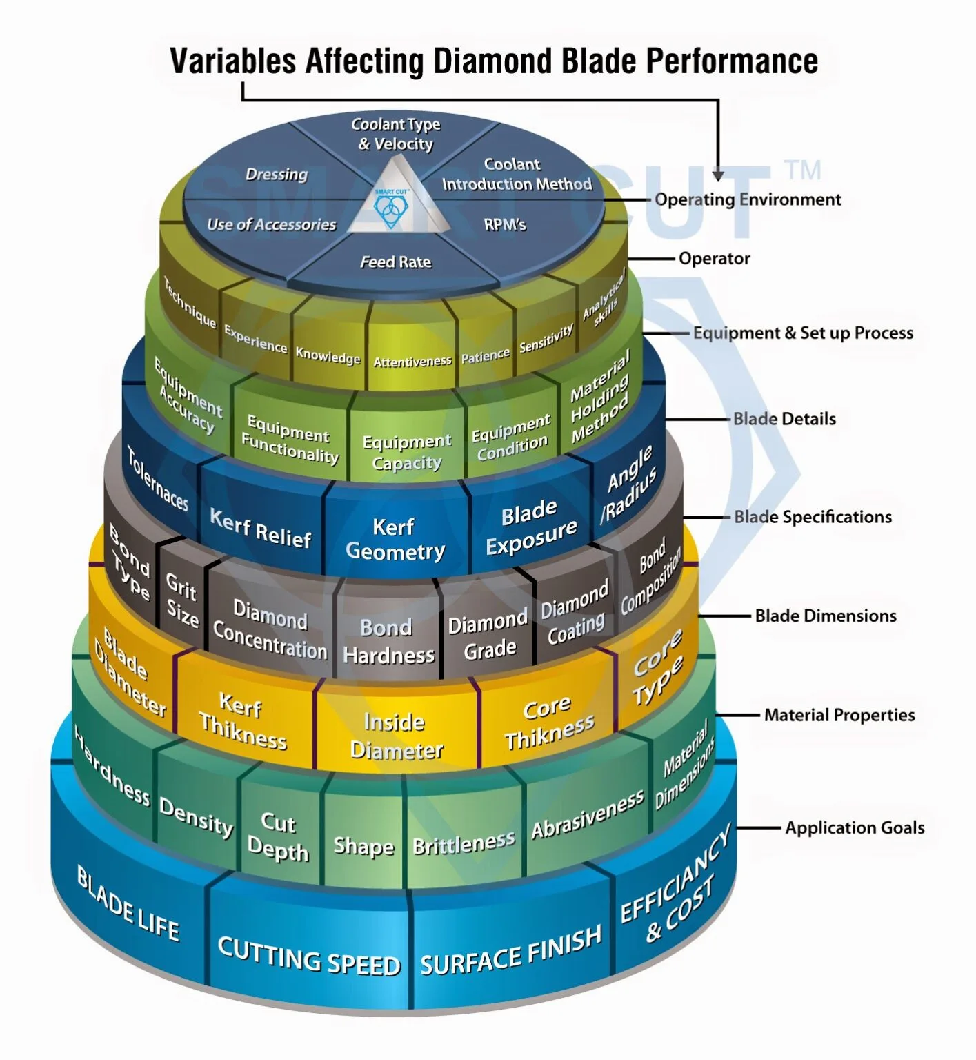
From a process engineering standpoint, blade dicing is characterized by direct physical contact between tool and wafer. This contact allows precise control over cutting depth and kerf width, but it also introduces mechanical stresses that must be carefully managed. The success of the blade dicing process depends on maintaining a stable balance between cutting efficiency and damage suppression throughout the entire wafer.
Unlike laser-based methods, blade dicing removes material physically rather than modifying internal stress fields. This makes the process highly adaptable to different wafer thicknesses, materials, and device layouts, provided that blade selection and process parameters are properly matched.
Steps in Wafer Blade Dicing
The blade dicing process consists of several sequential steps, each of which plays a specific role in controlling wafer integrity and final die quality. Although equipment automation has streamlined these steps, the underlying process logic remains unchanged.
Wafer Mounting and Alignment
The process begins with mounting the wafer onto dicing tape, which is typically a UV- or pressure-sensitive adhesive film supported by a metal or polymer frame. The tape provides mechanical support during cutting and prevents individual dies from separating prematurely. Proper mounting flatness is critical; any wafer warpage or trapped air can result in uneven cutting depth and localized chipping.
After mounting, the wafer is aligned using optical systems that detect alignment marks or scribe lines. Accurate alignment ensures that the blade follows the intended cutting paths and avoids active device regions. Misalignment at this stage cannot be corrected later and often results in catastrophic yield loss.
Blade Setup and Conditioning
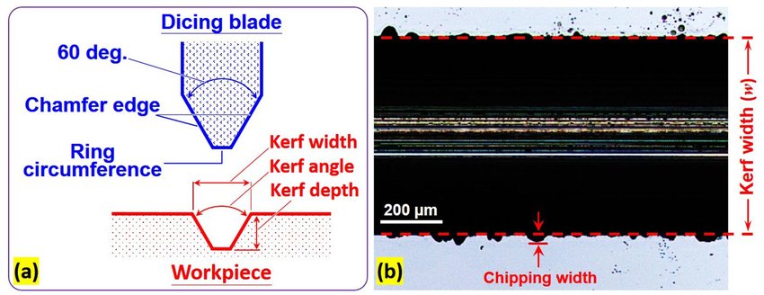
Before cutting begins, the dicing blade is installed, trued, and dressed if necessary. Blade conditioning ensures that diamond particles are properly exposed and that the blade rim is concentric with the spindle. Inconsistent blade exposure can lead to unstable cutting forces and non-uniform kerf widths across the wafer.
Blade setup must account for blade thickness, rim height, and expected wear behavior. These parameters are closely linked to the blade design described in dicing blade technology.
Cutting Pass Execution
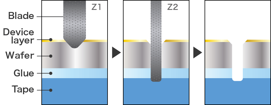
During the cutting pass, the blade rotates at high speed while feeding into the wafer at a controlled rate. Cutting depth is typically set to slightly exceed wafer thickness to ensure complete separation without excessive contact with the tape. Feed rate and spindle speed are selected to balance throughput and edge quality.
Cooling water or cutting fluid is continuously supplied to remove debris, dissipate heat, and stabilize cutting forces. Insufficient coolant flow can cause localized heating, accelerating bond degradation and increasing the risk of chipping.
Indexing and Full Wafer Singulation
After completing a set of parallel cuts in one direction, the wafer is indexed and rotated to perform orthogonal cuts. This step divides the wafer into individual dies while maintaining their position on the tape. Consistency between cutting directions is important, as anisotropic wafer properties can cause direction-dependent damage.
Typical Blade Dicing Process Parameters
Blade dicing performance is highly sensitive to process parameters. These parameters must be tuned as a system rather than independently adjusted.
| Parameter | Typical Range | Process Impact |
|---|---|---|
| Spindle Speed | 20,000–40,000 rpm | Affects cutting force, heat generation, and edge quality |
| Feed Rate | 1–10 mm/s | Controls throughput and risk of chipping |
| Cutting Depth | Wafer thickness + 5–20 µm | Ensures full cut-through without tape damage |
| Coolant Flow | Optimized per tool | Heat dissipation and debris removal |
Improper parameter selection often manifests as edge chipping, blade glazing, or premature blade wear. For this reason, parameter optimization must always be performed in conjunction with blade specification selection, such as thickness and width, discussed in dicing saw blade thickness and dicing saw blade width.
Blade Dicing vs Other Dicing Methods
From an engineering standpoint, blade dicing is one of several wafer singulation options. Each method occupies a distinct process window defined by material compatibility, cost, and damage mechanisms.
| Dicing Method | Material Removal | Damage Mechanism | Typical Use Case |
|---|---|---|---|
| Blade Dicing | Mechanical cutting | Chipping, micro-cracks | High-volume, multi-material wafers |
| Laser Dicing | Thermal ablation | Heat-affected zones | Thin wafers, selective applications |
| Stealth Dicing | Internal modification | Internal fracture control | Ultra-thin silicon wafers |
Blade dicing remains the preferred method where flexibility, cost control, and equipment availability are critical. Its compatibility with existing dicing saw platforms is discussed further in wafer dicing blades and equipment compatibility.
Typical Applications of Blade Dicing
Blade dicing is used across a wide spectrum of semiconductor applications, including logic ICs, memory devices, power semiconductors, MEMS, LEDs, and compound semiconductor wafers. Its adaptability allows engineers to tune blade technology and process parameters to match application-specific requirements.
For example, logic and memory devices emphasize kerf control and throughput, while power devices and compound semiconductors prioritize blade durability and edge integrity. These application-driven differences ultimately feed back into blade selection decisions outlined in How to Choose Dicing Blades.
Common Challenges in Blade Dicing
Despite its maturity, blade dicing presents several recurring challenges in production. Edge chipping is the most common issue and is typically caused by excessive cutting force, improper blade selection, or insufficient coolant flow. Subsurface damage may not be immediately visible but can degrade die strength and long-term reliability.
Blade wear and glazing can lead to unstable cutting behavior over time, requiring periodic blade dressing or replacement. Inconsistent wafer mounting or tape adhesion can introduce depth variation and incomplete cuts. Addressing these challenges requires a holistic approach that considers blade technology, process parameters, and equipment condition together.
A systematic approach to blade selection and process setup is discussed in detail in How to Choose the Right Dicing Blades, which builds directly on the process principles outlined on this page.
This concludes the process engineering overview of blade dicing. The next logical step is to examine the cutting tool itself in greater detail, starting with Diamond Dicing Blades for Precision Semiconductor Cutting.