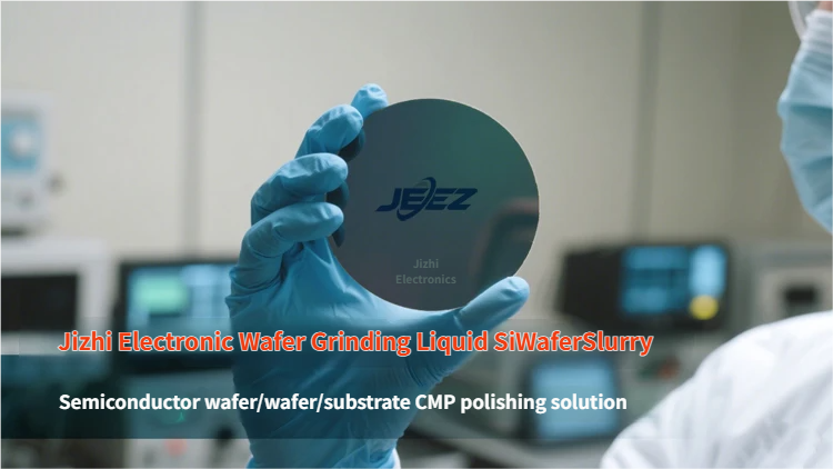
CMP Polishing Slurry for Electronic Silicon Wafers
I. CMP Polishing Technology: A Key Process in Semiconductor Manufacturing
Chemical Mechanical Planarization (CMP) is one of the core processes in semiconductor silicon wafer manufacturing, directly impacting chip performance and yield. During wafer processing, CMP achieves atomic-level surface planarization (roughness <0.2nm) through the synergistic action of chemical corrosion and mechanical grinding, meeting the ultra-clean and ultra-flat surface requirements of advanced process nodes.
Three Core Functions of Jizhi Electronics CMP Polishing Slurry
① Efficient Polishing: Nanoscale abrasives (e.g., colloidal SiO2) precisely remove surface protrusions, improving wafer flatness and reducing micro-scratches.
② Lubrication and Protection: Special additives reduce the coefficient of friction (<0.05), minimizing equipment wear and extending pad life.
③ Precise Temperature Control: High-thermal-conductivity fluid rapidly dissipates heat, preventing lattice damage caused by localized overheating.
II. Jizhi Electronics CMP Polishing Slurry: A Domestic High-End Alternative
Wuxi Jizhi Electronics Technology Co., Ltd. focuses on semiconductor material R&D. Its Silicon Wafer Polishing Slurry (Si Wafer Slurry) can serve as an alternative to imported slurries. It is suitable for the rough, intermediate, and fine polishing of 8-12 inch silicon wafers and reclaimed wafers, helping customers reduce production costs and improve process stability.
Technical Breakthroughs
① Highly Stable Nano-Abrasives: Utilizes surface modification technology with a Zeta potential > ±30mV, ensuring long-term slurry storage without sedimentation.
② Intelligent pH Control: Optimizes pH value for different polishing stages (rough → fine), reducing dishing (Dishing <5nm).
③ Low Defect Rate: Special chelating agents control metal impurities, achieving a defect density <0.1/cm², compatible with high-precision chip manufacturing.
III. Application Scenarios: Enabling High-Quality Semiconductor Manufacturing
Jizhi Electronics Semiconductor CMP Polishing Slurry is widely used in:
① Large Wafer Manufacturing: CMP planarization processing for 8-12 inch wafers.
② Reclaimed Wafers: Polishing recycled silicon wafers to lower production costs.
③ Advanced Packaging: Surface treatment for processes like TSV and 3D IC.
IV. Why Choose Jizhi Electronics Silicon Wafer Polishing Slurry?
① Domestic Alternative: Performance comparable to imported brands with significant price advantages.
② Customization Services: Formulas can be adjusted based on customer processes to optimize polishing efficiency.
③ Stable Supply: In-house production line ensures delivery timelines and reduces supply disruption risks.
With the rapid development of China’s semiconductor industry, the technological maturity and market acceptance of domestic CMP polishing slurries continue to rise. Leveraging advantages such as high polishing rate, ultra-low defect rate, and long service life, Jizhi Electronics has become a partner for domestic fabs and reclaimed silicon wafer companies.
For needs related to CMP slurry import substitution, silicon wafer grinding/polishing slurry, large-wafer polishing solutions, low-defect slurry, or CMP processes for reclaimed wafers, you may contact the Jizhi Electronics engineering team, available 24/7 to help you solve polishing challenges!