CMP Process Step-by-Step:How Wafer Polishing Works
A complete engineering walkthrough of every stage in the Chemical Mechanical Planarization process — from wafer loading and slurry delivery to endpoint detection and post-polish cleaning — with process parameters, control variables, and integration considerations.
CMP Process Overview
Chemical Mechanical Planarization (CMP) is a five-stage process that transforms a topographically rough wafer surface into a globally planar surface ready for the next photolithography step. Each stage is tightly coupled to the others: slurry chemistry must be matched to the polishing pad and process conditions; endpoint detection accuracy determines whether the wafer exits the tool at the correct thickness; and post-CMP cleaning effectiveness directly affects the defect density seen at the next inspection step.
This article is part of the JEEZ comprehensive resource on CMP technology. For the foundational overview of what CMP is and why it matters, see our CMP Semiconductor Complete Guide. Here we focus exclusively on the mechanics, physics, and engineering control of each individual process step.
Chemical Action
Reactive agents in the slurry modify the surface layer through oxidation, complexation, or pH-driven dissolution, reducing its mechanical hardness.
Mechanical Action
Abrasive nanoparticles, driven by relative velocity between wafer and pad under applied pressure, physically remove the chemically modified surface material.
In-Situ Metrology
Optical interferometry or motor-current sensing monitors film thickness in real time and signals the endpoint when target removal is reached.
Integrated Cleaning
An inline brush-scrub module removes residual particles and chemical by-products immediately after polishing, before the wafer can dry.
Step 1 — Substrate Preparation & Wafer Loading
Before polishing begins, the wafer must be securely and uniformly mounted in the carrier head — the rotating assembly that holds the wafer face-down against the polishing pad. Improper loading is a root cause of within-wafer non-uniformity (WIWNU) and edge exclusion defects, so this step receives significant engineering attention in production environments.
Carrier Head Architecture
A modern CMP carrier head consists of a rigid housing, a compliant membrane that presses the wafer backside, a retaining ring that confines the wafer laterally, and a backing film that distributes pressure evenly across the wafer surface. Multi-zone carrier heads — the industry standard at advanced nodes — divide the membrane into 5 to 7 independently controllable pressure zones, allowing the polishing downforce to be varied radially across the wafer to compensate for incoming thickness non-uniformity.
The retaining ring serves a critical function: it prevents the wafer from sliding out from under the carrier head and also influences the pressure distribution at the wafer edge. Retaining ring wear directly impacts edge die yield and must be monitored and replaced on a defined schedule. Retaining ring material (typically PEEK or PPS composite) and its groove pattern affect slurry distribution to the wafer edge region.
Backing Film Selection
The backing film is a compliant polymer sheet interposed between the rigid carrier membrane and the wafer backside. It serves two functions: distributing pressure uniformly over the wafer surface and providing a friction interface that transmits torque from the spinning carrier to the wafer. Backing film hardness represents a trade-off — softer films improve pressure uniformity but reduce polishing efficiency for thick film removal; harder films are preferred for precise endpoint control. Backing films have a defined replacement interval, typically 500–1,500 wafer passes, after which their compliance characteristics degrade.
Vacuum Hold-Down During Transfer
During transfer between the input cassette, the polishing station, and the cleaning module, the wafer is held by vacuum to prevent it from falling or contaminating its polished front surface. Loss of vacuum during transfer is a catastrophic event that must be detected and alarmed immediately. Transfer robot end-effectors are designed with edge-contact geometry to avoid touching the device surface.
Step 2 — Slurry Delivery
CMP slurry is the process consumable that most directly governs removal rate, selectivity, surface finish, and defect density. Slurry delivery to the polishing interface involves not only the chemical formulation but also the delivery method, flow rate, temperature, and point-of-use filtration system. For a comprehensive guide to slurry types and chemistry, refer to our article: CMP Slurry Guide: Types, Selection & Optimization.
Slurry Dispense Method
Slurry is dispensed from an overhead arm onto the rotating polishing pad surface, typically at a point 10–30 mm from the pad centre. Centrifugal force and pad rotation then distribute the slurry radially across the pad surface and into the pad-wafer contact zone. Flow rates typically range from 100 to 300 mL/min depending on pad size, rotation speed, and process requirements. Excessive flow wastes expensive slurry without proportional process benefit; insufficient flow causes slurry starvation at the wafer edge, increasing WIWNU.
Point-of-Use Filtration
Even slurries with a specification of <50 ppm large particles (>0.5 µm) can develop agglomerates during storage, transport, or delivery-line sitting. A point-of-use (POU) in-line filter — typically 1–5 µm absolute rating — is installed at the tool slurry inlet to capture agglomerates before they reach the wafer. POU filters must be changed on schedule; a clogged or bypassed POU filter is one of the most common root causes of sudden scratch-defect excursions. See our article on CMP defect types and yield improvement for more on slurry-driven scratch mechanisms.
Slurry Temperature Control
Slurry temperature affects chemical reaction rates and thus removal rate. Many CMP processes are temperature-sensitive: a 5°C rise in slurry temperature can increase removal rate by 10–15% for oxide CMP. Most production tools include a slurry temperature control system (chiller/heater) to maintain ±1°C stability. Slurry should also be protected from freezing — a single freeze-thaw cycle can irreversibly agglomerate colloidal abrasive particles, rendering the slurry unsuitable for production use.
Step 3 — Mechanical Polishing
The polishing step is where material removal actually occurs. The wafer, mounted face-down in the carrier head, is pressed against the rotating polishing pad while the carrier itself rotates. The relative velocity between the wafer surface and the pad surface — combined with the chemical action of the slurry — drives the material removal mechanism.
Preston’s Equation: The Fundamental Relationship
The material removal rate (MRR) in CMP is approximated by Preston’s equation:
where Kp is the Preston coefficient (a material- and chemistry-dependent constant), P is the applied downforce pressure (psi or kPa), and V is the relative velocity between wafer and pad (m/s). This relationship shows that both pressure and velocity can be used to control removal rate, and that their product — often called the “PV product” — is the primary mechanical process lever.
In practice, however, CMP does not follow Preston’s equation perfectly. At very high pressures, the relationship becomes sub-linear because the pad asperities are compressed and the contact area increases non-linearly. At very low pressures, removal rate drops off more steeply than expected as chemical reaction-limited kinetics dominate. The practical operating window for most production CMP processes is 1–6 psi downforce with platen speeds of 30–100 RPM.
Pad Rotation and Kinematics
On a conventional rotary CMP tool, both the platen (carrying the pad) and the carrier head rotate independently. The carrier head also oscillates radially — sweeping back and forth across the pad radius — to ensure uniform pad utilisation and slurry distribution. The combination of platen rotation, carrier rotation, and carrier sweep creates a complex velocity field at the wafer surface. Process engineers must characterise this velocity field to understand within-wafer removal rate patterns and design multi-zone pressure profiles that compensate for them.
Polishing Pad Role
The polishing pad is the second critical consumable in CMP. Its surface asperities transport slurry to the polishing interface and its bulk mechanical properties determine how pressure is distributed across the wafer. A new pad must be “broken in” through a conditioning procedure before it delivers stable, reproducible removal rates. Pad glazing — the progressive smoothing of pad asperities with wafer passes — causes removal rate drift and must be counteracted by in-situ pad conditioning. For full details on pad selection and conditioning, see: CMP Polishing Pad: Types, Selection & Performance Guide.
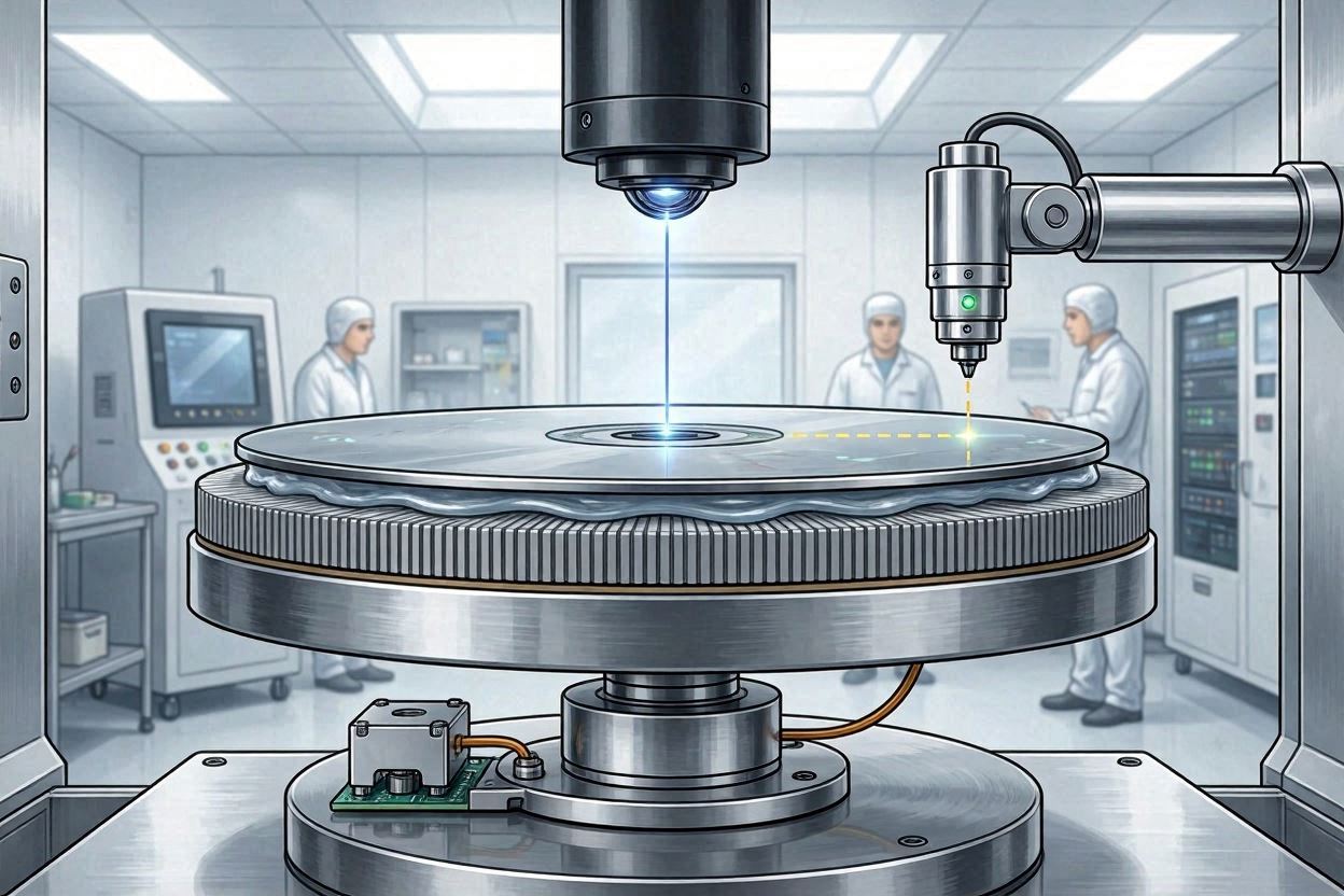
Step 4 — Endpoint Detection
Endpoint detection is the real-time measurement system that tells the CMP tool when to stop polishing. Stopping too early leaves excess material (under-polish); stopping too late removes material below the target layer (over-polish, dishing, or stop-layer erosion). At advanced nodes, the endpoint window can be as narrow as ±3 nm — requiring sub-nanometre resolution in real-time film thickness measurement.
Optical Interferometry (In-Situ Reflectometry)
The most widely used endpoint method for dielectric and metal CMP is optical interferometry. A transparent window in the polishing pad allows a laser beam to illuminate the wafer surface through the slurry layer. The reflected signal carries interference information that enables real-time calculation of film thickness at one or more points across the wafer. As the film thins during polishing, the interference signal oscillates with a period determined by the film’s refractive index and the polishing wavelength. The endpoint is triggered when the signal reaches a pre-determined threshold corresponding to the target film thickness.
Modern tools use broadband spectrometric reflectometry rather than single-wavelength interferometry, allowing simultaneous measurement at multiple wavelengths. This improves accuracy and enables thickness measurement of multi-layer film stacks — essential for advanced-node processes where CMP is stopping within a thin barrier metal layer above a critical device structure.
Motor Current Endpoint
An alternative endpoint method — particularly useful for metal CMP — monitors the current drawn by the platen or carrier head motor. As polishing transitions from a soft overlayer (e.g., copper) to a harder underlayer (e.g., tantalum barrier or oxide stop layer), the friction force changes, causing a detectable shift in motor current. This method is simpler and requires no pad window, but it is less precise than optical methods and is sensitive to process drifts unrelated to film thickness.
Multi-Zone Closed-Loop Control
The real power of modern endpoint systems lies not just in detecting when to stop, but in enabling active, real-time thickness control across the wafer during polishing. By combining in-situ thickness measurements at multiple radial positions with multi-zone carrier head pressure control, the tool can dynamically adjust the removal rate profile to flatten incoming thickness gradients. This closed-loop approach routinely achieves WIWNU below 1% — and at advanced nodes, below 0.3% — across 300 mm wafers.
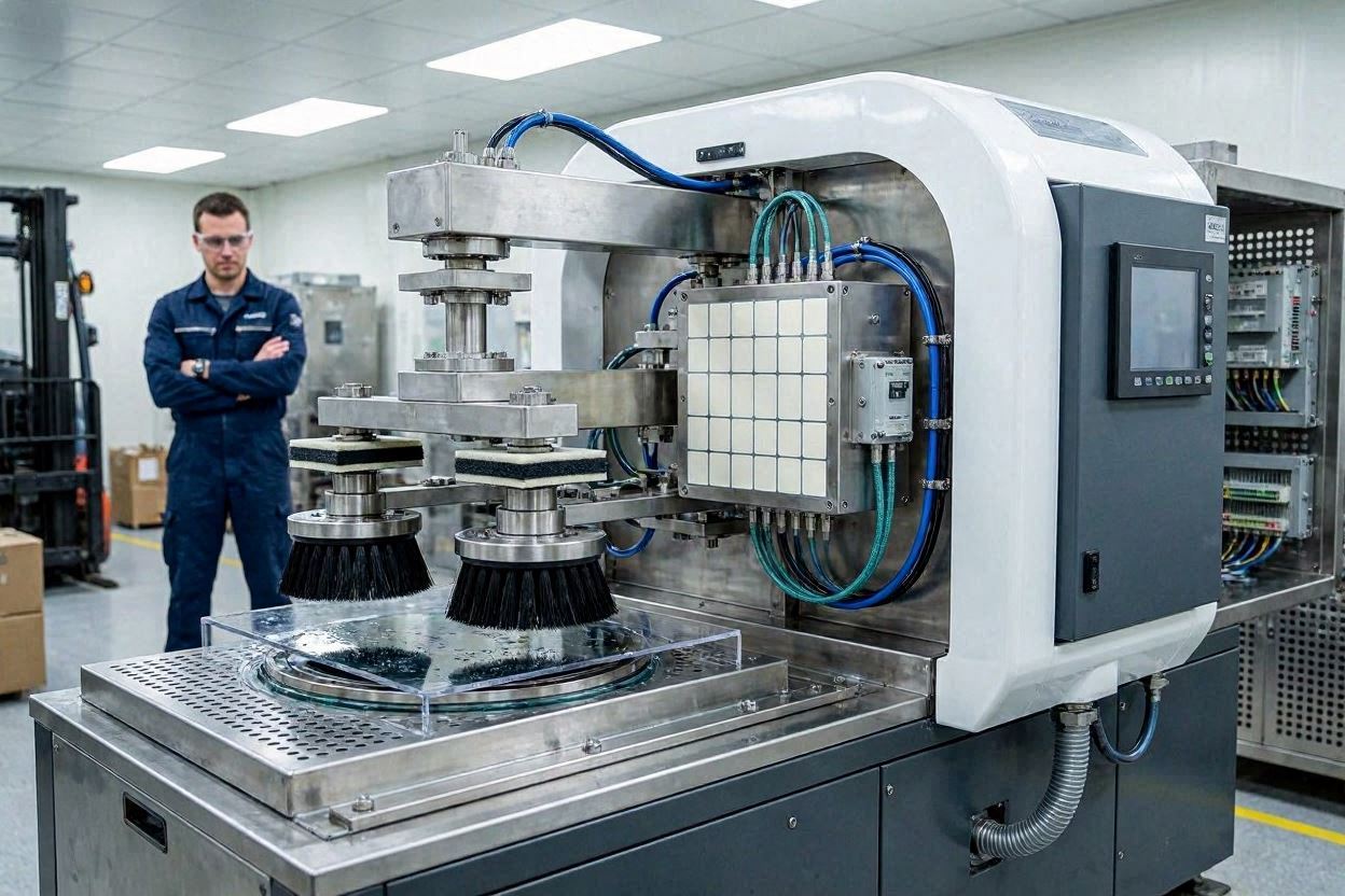
Step 5 — Post-CMP Cleaning
Immediately after polishing, the wafer surface is contaminated with residual slurry particles, polishing reaction by-products, dissolved metal ions, and organic residues. If allowed to dry, many of these contaminants become extremely difficult to remove. Post-CMP cleaning must therefore begin within seconds of polishing completion — before the slurry film on the wafer surface evaporates.
For the full engineering treatment of post-CMP cleaning chemistry and methods, see our dedicated article: Post-CMP Cleaning: Methods, Challenges & Best Practices. In summary, the cleaning module typically performs: (1) an initial rinse to dilute bulk slurry, (2) brush scrub cleaning with pH-controlled cleaning chemistry on both wafer faces, (3) a second clean with DI water, and (4) spin-rinse-dry (SRD) before the wafer exits the CMP module.
Key Process Parameters & Their Effects
| Parameter | Typical Range | Effect on MRR | Effect on Defects |
|---|---|---|---|
| Downforce (pressure) | 1 – 6 psi | ↑ pressure → ↑ MRR (Preston) | ↑ pressure → ↑ scratch risk |
| Platen speed | 30 – 120 RPM | ↑ speed → ↑ MRR | ↑ speed → ↑ slurry throw-off, ↓ slurry residence time |
| Slurry flow rate | 100 – 300 mL/min | ↓ below threshold → ↓ MRR at edge | ↑ flow → ↓ slurry starvation; ↑ particle residue if too high |
| Slurry temperature | 20 – 30 °C | ↑ temp → ↑ chemical MRR | ↑ temp → ↑ corrosion risk (Cu CMP) |
| Pad conditioning | In-situ continuous | Active conditioning maintains stable MRR | Over-conditioning → ↑ pad particle generation |
| Carrier head pressure zones | 5 – 7 zones, 0.5 – 6 psi each | Zone profile controls WIWNU | Non-uniform pressure → WIWNU, edge defects |
CMP Applications: FEOL, MOL & BEOL
CMP is used at every stage of the IC manufacturing flow. Understanding which specific CMP step you are working with — front-end-of-line (FEOL), middle-of-line (MOL), or back-end-of-line (BEOL) — is essential because the target material, process requirements, and defect sensitivities differ dramatically between them.
- FEOL CMP: Primarily STI oxide CMP using ceria-based slurries. Nitride stop layer selectivity is paramount. Scratch defects at this stage can directly damage transistor gate regions. Any contamination at FEOL — particularly metallic — is catastrophic for device performance.
- MOL CMP: Tungsten (W) CMP for contact plugs; increasingly cobalt (Co) CMP at 7 nm and below. Alumina-based slurries for tungsten. High removal rate is required to clear field tungsten without excessive oxide loss.
- BEOL CMP: Multiple Cu CMP steps per metal layer in the dual-damascene interconnect stack, plus barrier metal (TaN/Ta) CMP, and ILD (low-k dielectric) polishing. Copper dishing, dielectric erosion, and corrosion are the primary yield detractors. As metal layers approach M0 and M1 at sub-5 nm, cobalt and ruthenium local interconnects require new BEOL CMP process modules.
Common CMP Process Issues & Fixes
Process issue diagnosis
Most CMP process problems fall into one of four categories: removal rate drift, within-wafer non-uniformity, defect excursions, or post-clean contamination. Understanding the root cause mechanism is the only reliable path to a durable corrective action. See our dedicated guide: CMP Defect Types, Root Causes & Yield Improvement.
- Removal rate drift (decreasing over time): Usually caused by pad glazing. Verify pad conditioner disk condition and conditioning recipe. Increase conditioning aggressiveness or frequency. Check for slurry dispensing arm drift causing starvation at the pad edge.
- High centre-to-edge non-uniformity: Usually caused by retaining ring wear, incorrect multi-zone pressure profile, or backing film degradation. Measure carrier head pressure map and adjust zone recipe. Check retaining ring height and replace if worn beyond spec.
- Scratch excursion: Check POU filter — replace if at end of life. Pull slurry lot sample for LPC analysis. Inspect pad for embedded particles or surface damage. Review slurry dilution ratio and mixing system.
- Post-CMP particle residue: Review cleaning chemistry pH vs. target film surface charge (zeta potential alignment). Verify brush contact force and brush condition. Check cleaning chemistry flow rate and temperature. Review rinse water quality (TOC, resistivity).
- Copper dishing above spec: Reduce over-polish time. Review slurry corrosion inhibitor concentration. Evaluate pad hardness — stiffer pad reduces dishing in wide features. Check endpoint detection sensitivity.
Need CMP Consumables for Your Process?
JEEZ supplies CMP polishing slurries and pads to fabs worldwide. Contact our technical team to discuss your process requirements.
Contact JEEZ →