Copper CMP Slurry for Advanced Semiconductor Manufacturing
1. Introduction to Copper CMP
Copper has become the dominant interconnect material in advanced semiconductor devices due to its low resistivity and superior electromigration resistance compared to aluminum. However, copper cannot be patterned by conventional plasma etching, making Chemical Mechanical Planarization (CMP) an indispensable step in copper damascene integration.
Copper CMP slurry is not merely a consumable material; it is an active chemical system that directly defines removal rate, selectivity, defectivity, and long-term yield stability.
Unlike oxide CMP, copper CMP involves strong electrochemical interactions, corrosion risks, and complex surface passivation phenomena, making slurry formulation significantly more challenging.
For an overview of CMP slurry fundamentals, refer to:
CMP Slurry for Semiconductor Manufacturing
2. Role of Copper CMP Slurry in BEOL Integration
In a typical copper dual-damascene process, CMP slurry must fulfill multiple competing requirements:
- Efficient removal of excess copper overburden
- High selectivity to dielectric and barrier layers
- Suppression of corrosion and galvanic attack
- Minimization of dishing and erosion
Copper CMP slurry performance directly impacts:
- Line resistance variation
- Interconnect reliability
- Via resistance and electromigration lifetime
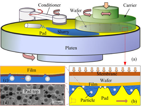
3. Chemical–Mechanical Removal Mechanism
Copper CMP is governed by a synergistic chemical–mechanical mechanism rather than pure abrasion.
3.1 Chemical Oxidation
Oxidizers such as hydrogen peroxide convert metallic copper into a softer oxide or hydroxide layer:
Cu → Cu+ / Cu2+ → CuO / Cu(OH)2
3.2 Complexation & Dissolution
Complexing agents stabilize dissolved copper ions and prevent redeposition onto the wafer surface.
3.3 Mechanical Removal
Abrasive particles and polishing pad asperities mechanically remove the chemically modified copper layer.
4. Copper CMP Slurry Composition Architecture
4.1 Abrasive System
Colloidal silica is the most widely used abrasive due to its low scratch propensity and controllable surface chemistry.
4.2 Oxidizers
- Hydrogen peroxide (H2O2)
- Ferric nitrate (less common)
4.3 Complexing Agents
- Glycine
- Citric acid
- Ammonium salts
4.4 Corrosion Inhibitors
Benzotriazole (BTA) is the most widely used inhibitor, forming a protective Cu–BTA complex layer.
5. Two-Step Copper CMP Slurry Systems
Modern copper CMP typically adopts a two-step slurry approach:
5.1 Bulk Copper Removal Slurry
- High oxidizer concentration
- High MRR
- Primary goal: throughput
5.2 Copper Buff / Barrier Slurry
- Low oxidizer concentration
- High selectivity
- Primary goal: surface quality
| Parameter | Bulk Cu Slurry | Cu Buff Slurry |
|---|---|---|
| MRR (nm/min) | 300–800 | 50–150 |
| Dishing (nm) | < 40 | < 15 |
| Oxidizer (wt%) | 1–5 | < 1 |
6. Key Engineering Parameters & Data Ranges
| Metric | Typical Range | Engineering Significance |
|---|---|---|
| pH | 3.5–6.0 | Controls corrosion vs MRR |
| Zeta Potential (mV) | -30 to -50 | Slurry stability |
| Scratch Density | < 0.1 / wafer | Yield impact |
7. Process Window & Control Maps
8. Defect Mechanisms & Root Cause Analysis
8.1 Dishing
Occurs due to differential removal rate between copper lines and surrounding dielectric.
8.2 Corrosion & Pitting
Typically caused by insufficient inhibitor coverage or excessive oxidizer concentration.
8.3 Scratches
Driven by abrasive PSD tail and slurry agglomeration.
9. High-Volume Manufacturing (HVM) Challenges
Many copper CMP slurries perform well at R&D scale but fail under HVM conditions due to:
- Shear-induced agglomeration
- Filter loading effects
- Tool-to-tool variability
Robust copper CMP slurry must demonstrate stable performance over extended recirculation periods.
10. Slurry Selection & Optimization Guidelines
- Define priority: throughput vs surface quality
- Match slurry chemistry with polishing pad
- Validate corrosion margin under worst-case conditions
11. Future Trends in Copper CMP Slurry
Future copper CMP slurry development focuses on:
- Lower defectivity for sub-5 nm nodes
- Reduced environmental impact
- Compatibility with hybrid bonding processes