Diamond Dicing Blades for Semiconductor Wafers
Diamond dicing blades for wafers are not generic cutting tools; they are highly engineered consumables designed to meet the mechanical, thermal, and material-specific requirements of semiconductor wafer singulation. As wafer materials diversify from traditional silicon to compound semiconductors such as SiC, GaAs, GaN, and InP, the performance demands placed on diamond dicing blades have become significantly more complex. Blade selection now directly affects die strength, edge chipping, kerf loss, thermal damage, and overall yield.
This page focuses on how wafer material properties drive different technical requirements for diamond dicing blades. It serves as an application-level extension of the core wafer dicing blades pillar page, providing deeper insight into blade design logic for silicon and compound semiconductor wafers.
Table of Contents
- Requirements for Wafer Dicing Blades
- Diamond Dicing Blades for Silicon Wafers
- Diamond Dicing Blades for Compound Semiconductors
- Performance Considerations in Wafer Dicing
Requirements for Wafer Dicing Blades
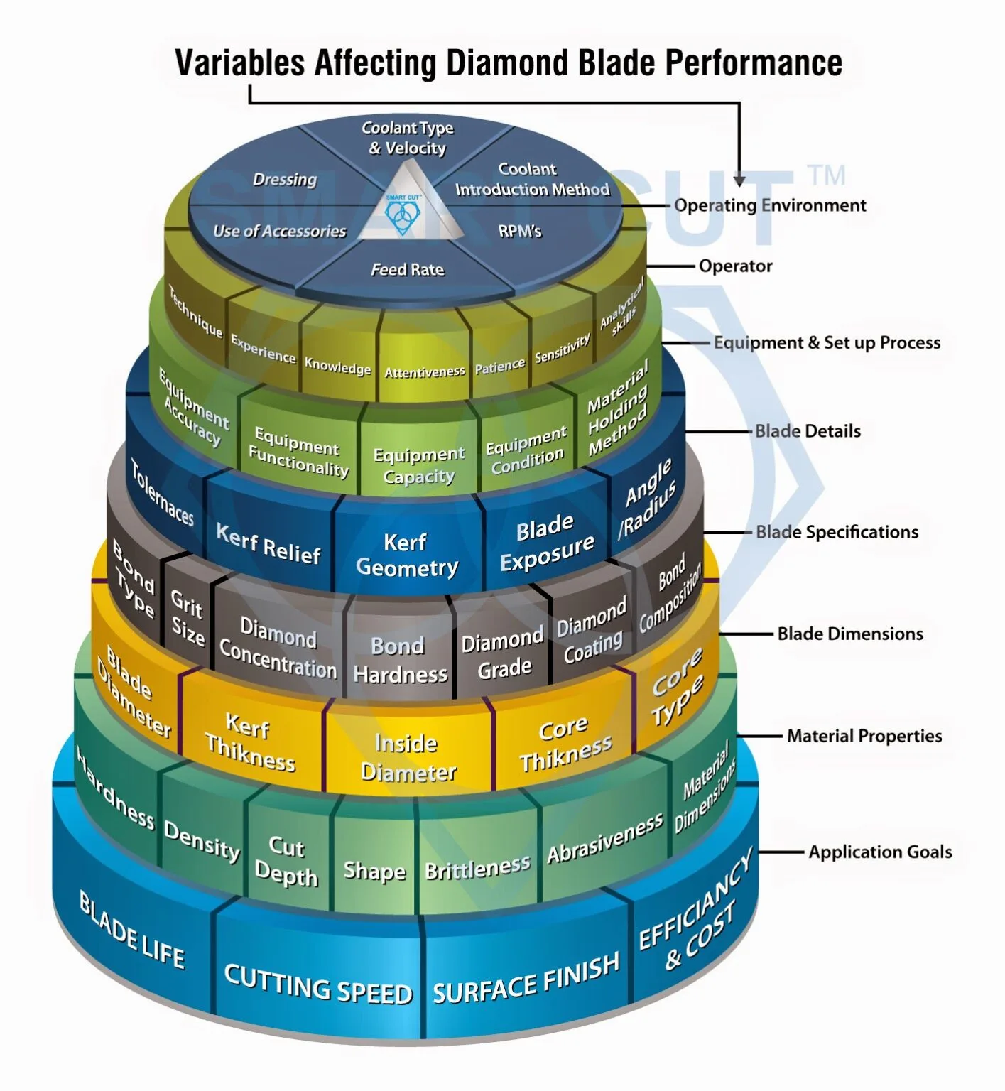
Wafer dicing blades must satisfy a combination of mechanical precision, material compatibility, and process stability. Unlike general cutting tools, the blade must operate within micrometer-level tolerances while minimizing subsurface damage and thermal stress.
Key functional requirements include:
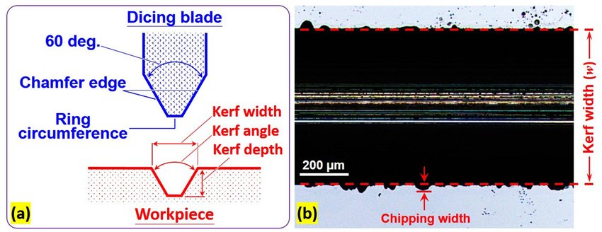
- Consistent kerf width control to reduce die size variation
- Low edge chipping to maintain die mechanical strength
- Minimal subsurface microcracking
- Stable cutting force throughout blade life
- Controlled wear rate to avoid frequent blade dressing
- Compatibility with high-speed spindle systems (30,000–60,000 rpm)
These requirements are directly influenced by wafer hardness, fracture toughness, thermal conductivity, and crystal structure. Therefore, blade design parameters such as diamond grit size, concentration, bond type, and blade thickness must be tailored to the wafer material.
| Parameter | Impact on Wafer Dicing |
|---|---|
| Diamond Grit Size | Affects surface finish, cutting force, and edge chipping |
| Diamond Concentration | Controls blade life and cutting stability |
| Bond Type | Determines diamond retention and self-sharpening behavior |
| Blade Thickness | Directly impacts kerf loss and die density |
| Blade Stiffness | Influences cut straightness and vibration resistance |
Diamond Dicing Blades for Silicon Wafers
Silicon remains the dominant wafer material in semiconductor manufacturing. Although silicon is relatively brittle, it has well-understood mechanical properties and comparatively low hardness, making it more forgiving in dicing operations than most compound semiconductors.
Material Characteristics of Silicon Wafers
- Mohs hardness: ~6.5–7
- Fracture toughness: moderate
- Thermal conductivity: high
- Crystal structure: diamond cubic
These properties allow silicon wafers to be diced efficiently with resin-bond or hybrid-bond diamond blades optimized for low chipping and high throughput.
Typical Blade Design for Silicon Wafer Dicing
For silicon wafers, the primary objective is balancing cutting speed with edge quality. Blade designs typically emphasize fine diamond grit and moderate concentration to reduce brittle fracture at the cut edge.
| Blade Parameter | Typical Range for Silicon |
|---|---|
| Diamond Grit Size | #2000 – #4000 |
| Diamond Concentration | Low to medium |
| Bond Type | Resin bond or resin-metal hybrid |
| Blade Thickness | 20–50 μm |
| Spindle Speed | 30,000–40,000 rpm |
Resin-bond blades are commonly used because they offer excellent self-sharpening behavior and reduced cutting force, which helps minimize edge chipping on silicon dies.
Common Failure Modes in Silicon Dicing
- Edge chipping due to excessive feed rate
- Blade glazing caused by insufficient dressing
- Kerf widening from uneven blade wear
These issues are typically process-related rather than material-limited, making silicon wafer dicing more controllable compared to compound semiconductors.
Diamond Dicing Blades for Compound Semiconductors
Compound semiconductor wafers introduce significantly higher cutting difficulty. Materials such as silicon carbide (SiC), gallium nitride (GaN), gallium arsenide (GaAs), and indium phosphide (InP) exhibit higher hardness, lower fracture toughness, or anisotropic crystal behavior, which places much higher demands on diamond dicing blade performance.
Material Property Comparison
| Material | Hardness | Fracture Behavior | Dicing Difficulty |
|---|---|---|---|
| Silicon (Si) | Medium | Brittle but predictable | Low |
| Silicon Carbide (SiC) | Very high | Brittle, high cutting force | Very high |
| Gallium Nitride (GaN) | High | Prone to microcracks | High |
| Gallium Arsenide (GaAs) | Medium | Cleavage-sensitive | Medium |
| Indium Phosphide (InP) | Low-medium | Very brittle | Medium |
Blade Design Challenges for Compound Semiconductors
Compound semiconductor wafers require blades with higher diamond exposure, stronger bonding, and improved stiffness to maintain cutting stability. Metal bond or vitrified bond diamond blades are more commonly used due to their superior diamond retention and wear resistance.
| Blade Parameter | Typical Range for Compound Semiconductors |
|---|---|
| Diamond Grit Size | #800 – #2000 |
| Diamond Concentration | Medium to high |
| Bond Type | Metal bond or vitrified bond |
| Blade Thickness | 30–80 μm |
| Spindle Speed | 20,000–35,000 rpm |
Special Considerations for SiC and GaN
For SiC and GaN wafers, blade wear rate and thermal damage become critical limiting factors. Excessive cutting force can cause subsurface cracking that propagates during subsequent packaging or thermal cycling.
Engineering strategies often include:
- Using coarser diamond grit to reduce cutting force
- Increasing coolant flow to manage heat
- Reducing feed rate to improve cut stability
- Implementing frequent blade dressing cycles
Performance Considerations in Wafer Dicing
Regardless of wafer material, diamond dicing blade performance must be evaluated holistically rather than by a single parameter. Key performance indicators include blade life, cut quality consistency, and process window stability.
Key Performance Metrics
- Edge chipping size (μm)
- Kerf width variation
- Blade wear rate (μm per meter)
- Subsurface damage depth
- Die breakage rate
Optimizing these metrics requires coordination between blade design, machine setup, and process parameters. Detailed blade selection principles are discussed in the guide How to Choose Dicing Blades, which complements this wafer-focused analysis.
Core Technology
Understanding wafer-specific blade requirements also depends on the underlying blade structure and bonding mechanisms. For readers seeking a deeper technical foundation, refer back to Dicing Blade Technology in Semiconductor Manufacturing and the main wafer dicing blades overview.
By aligning diamond dicing blade design with wafer material properties, semiconductor manufacturers can significantly improve yield, reduce process variability, and extend blade service life in advanced wafer dicing applications.