Dicing Saw Blade Width in Semiconductor Dicing
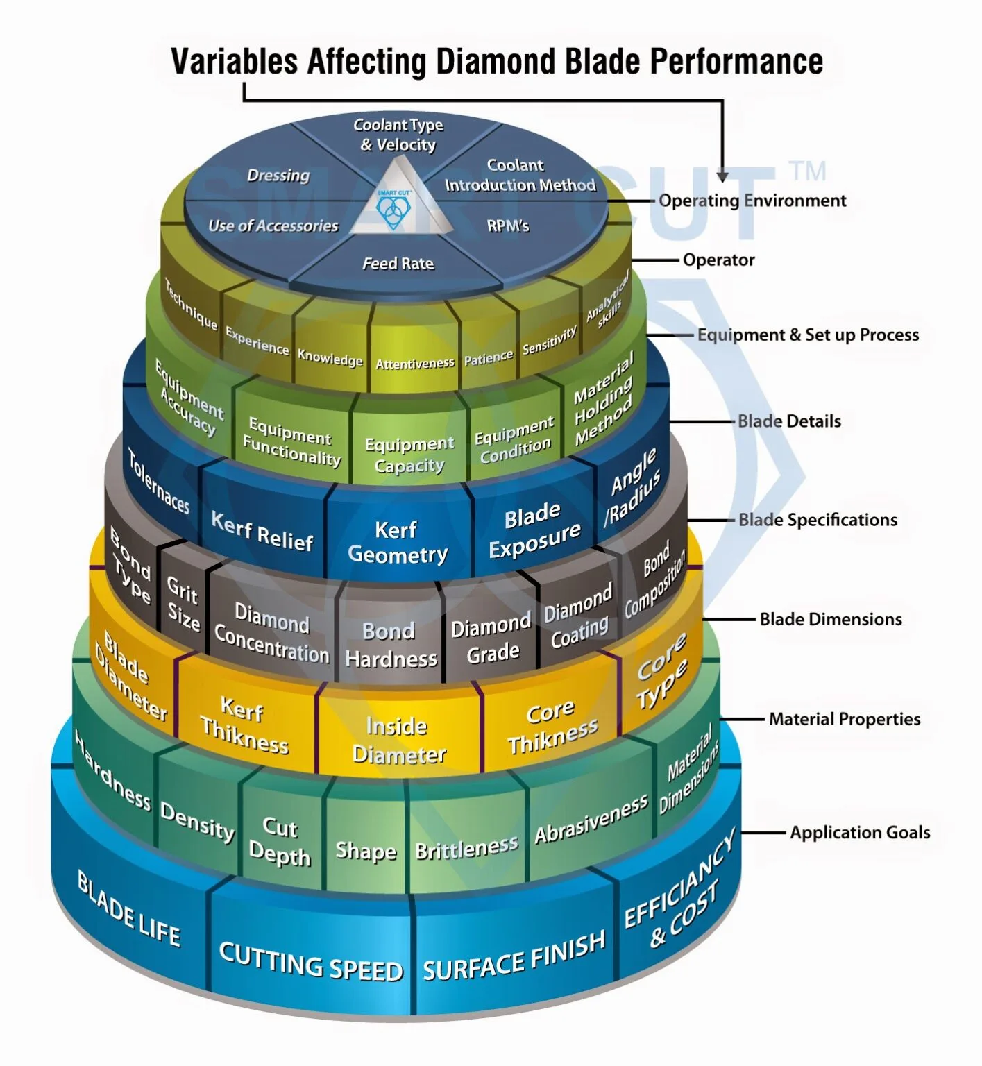
Dicing saw blade width is a critical parameter that directly determines kerf control, cutting precision, and blade path stability during wafer dicing. Although blade width is often discussed together with blade thickness, from an engineering perspective these two parameters serve different functional roles. Blade thickness primarily governs structural stiffness and kerf loss, while blade width defines the effective cutting envelope and amplifies or suppresses positional and dynamic errors during cutting.
This page provides a detailed engineering-level explanation of dicing saw blade width, focusing on how width affects kerf consistency, die dimensional accuracy, and walking stability during linear dicing. It complements the wafer dicing blades pillar page and should be read together with Dicing Saw Blade Thickness and Wafer Dicing Blades Equipment.
Table of Contents
- Definition of Dicing Blade Width
- Blade Width vs Cutting Precision
- Kerf Width Optimization
- Blade Width Selection Guidelines
Definition of Dicing Blade Width
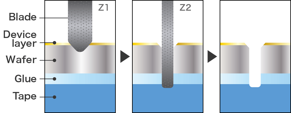
Dicing blade width refers to the effective lateral cutting dimension of the blade during operation. Unlike nominal blade thickness, which is a geometric property measured at rest, blade width reflects the actual material removal envelope during cutting.
In practical wafer dicing, effective blade width includes:
- Nominal blade thickness
- Diamond grit protrusion on both sides
- Elastic blade deflection under cutting load
- Spindle runout and dynamic vibration
As a result, blade width should be treated as a dynamic process parameter rather than a fixed geometric value. Two blades with identical nominal thickness can exhibit different effective cutting widths depending on bond type, diamond exposure, and equipment rigidity.
Nominal Thickness vs Effective Cutting Width
| Parameter | Description |
|---|---|
| Nominal Thickness | Measured blade thickness at rest |
| Diamond Protrusion | Exposed diamond height contributing to cutting |
| Effective Blade Width | Total lateral cutting envelope during dicing |
Understanding this distinction is essential for accurate kerf control and die size prediction.
Blade Width vs Cutting Precision
Cutting precision in wafer dicing refers to the ability of the blade to follow the programmed cut path without lateral deviation, waviness, or oscillation. Blade width plays a central role in how mechanical and dynamic errors are translated into kerf variation.
Error Amplification Mechanism
Wider effective blade widths increase sensitivity to spindle runout and vibration. Any lateral displacement of the blade centerline is directly transferred to the cut edge, enlarging kerf width variation and degrading die dimensional accuracy.
Key sources of lateral error include:
- Spindle radial runout
- Blade imbalance
- Asymmetric diamond wear
- Uneven flange clamping
| Error Source | Effect on Narrow Blade | Effect on Wide Blade |
|---|---|---|
| Radial runout | Minor kerf variation | Significant kerf widening |
| Vibration | Localized chipping | Kerf waviness |
| Diamond wear asymmetry | Gradual drift | Rapid cut deviation |
This is why advanced dicing processes often prioritize narrow and stable blade widths rather than simply minimizing nominal thickness.
Blade Walking and Path Stability
Blade walking refers to the gradual lateral drift of the blade during long cuts. This phenomenon is closely related to blade width and wear symmetry. Wider blades generate higher lateral cutting forces, increasing the risk of directional instability.
Blade walking is more pronounced in:
- Long continuous cuts across large wafers
- High feed rate operations
- Hard or anisotropic wafer materials
Controlling blade width and ensuring symmetric diamond distribution are critical to maintaining path stability.
Kerf Width Optimization
Kerf width optimization aims to achieve the narrowest possible and most consistent kerf without compromising cutting stability or die strength. Blade width is the dominant contributor to kerf geometry.
Components of Kerf Width
- Effective blade width
- Dynamic lateral motion
- Thermal expansion effects
- Debris evacuation efficiency
Reducing nominal blade thickness alone does not guarantee kerf reduction if blade width increases due to instability.
| Blade Design | Nominal Thickness | Typical Kerf Width |
|---|---|---|
| Thin, unstable blade | 20 μm | 26–30 μm |
| Optimized narrow-width blade | 25 μm | 27–29 μm |
| Wide, rigid blade | 40 μm | 42–48 μm |
From a yield perspective, kerf consistency is often more valuable than absolute kerf minimization.
Interaction with Die Strength
Blade width also affects die edge quality. Wider cutting envelopes increase the probability of microchipping and subsurface damage due to higher lateral stress. These defects may not be visible immediately but can significantly reduce die mechanical strength.
Maintaining a narrow and stable blade width reduces stress concentration at the cut edge, improving downstream reliability.
Blade Width Selection Guidelines
Blade width selection should follow a structured approach that integrates wafer material properties, die layout requirements, and equipment capability.
Engineering Selection Principles
- Select the narrowest blade width that remains dynamically stable
- Avoid over-reliance on nominal thickness specifications
- Match blade width to spindle runout and rigidity
- Validate kerf stability over full blade life
Typical Blade Width Ranges
| Application | Recommended Blade Width |
|---|---|
| Standard silicon wafers | 22–30 μm |
| High-density die layouts | 20–25 μm |
| SiC / GaN wafers | 35–60 μm |
| Thick power device wafers | 50–80 μm |
Equipment Constraint Check
Equipment limitations often dictate a minimum achievable blade width. High spindle runout or insufficient flange stiffness requires wider blades to maintain stability.
For a comprehensive selection strategy that integrates blade width with thickness, bond type, and wafer material, refer to How to Choose Dicing Blades.
System-Level Understanding
Blade width optimization cannot be isolated from blade thickness and equipment dynamics. Readers are encouraged to review Dicing Saw Blade Thickness for stiffness considerations and Wafer Dicing Blades Equipment for spindle and flange constraints.
By treating blade width as a dynamic process variable rather than a static specification, semiconductor manufacturers can achieve superior kerf control, improved die accuracy, and stable long-term dicing performance.