How Polishing Template Edge Design Controls Wafer Edge Profile & Reduces Edge Exclusion
Every millimeter of edge exclusion zone you eliminate converts directly into additional die area. This guide explains the physics of edge rolloff and the template design parameters that control it — including how sub-2 mm edge exclusion is achieved at scale.
Why Edge Exclusion Is a Yield Problem Worth Engineering For
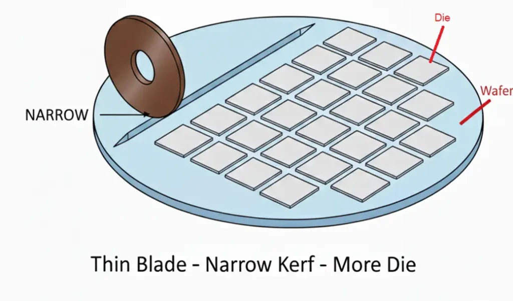
Edge exclusion is defined by SEMI Standard M49 as the annular zone at the wafer perimeter within which die sites are not counted for yield because the surface flatness or layer thickness at those locations falls outside specification. At 300 mm with a 3 mm edge exclusion zone, approximately 3.8% of the wafer area is excluded — an area that could yield additional die on every wafer processed. At 150 mm with a 5 mm edge exclusion zone, over 12% of wafer area is excluded.
For advanced logic and memory devices where die size is small and die-per-wafer counts are high, reducing edge exclusion from 3 mm to 1.5 mm on a 300 mm wafer recovers approximately 1.9% of wafer area — which at a die yield of 90% and a selling price of $100 per die translates directly to additional revenue on every wafer shipped. Across a production line running 10,000 wafers per month, even a 1% recovery in die-per-wafer count represents significant annual revenue impact.
The edge exclusion zone is set by the polishing process, not the wafer specification: it is the zone where edge rolloff makes the polished surface too non-flat to meet the flatness specification required for successful photolithography. Reducing edge exclusion therefore requires reducing edge rolloff — and edge rolloff is controlled, to a significant degree, by the polishing template edge design. Understanding the full mechanics of how polishing templates work establishes the foundation for understanding why edge geometry matters.
The Physics of Edge Rolloff
Edge rolloff is a mechanical consequence of the polishing pad’s elastic behavior at the wafer perimeter. During polishing, the wafer sits face-down on the rotating polishing pad, with the wafer backside held against the template’s backing pad. The polishing pad contacts the wafer front face across the full wafer area and then must transition — at the wafer edge — to a zone where there is no longer a solid substrate beneath it.
At this transition point, the polishing pad deflects downward under its own elastic bending stiffness and the difference in support between the wafer area (rigid, backed by the wafer itself and the template) and the annular gap zone (compliant, backed only by the polishing pad’s bending resistance). This downward deflection of the pad at the wafer perimeter reduces the local contact pressure between the pad and the wafer surface in a zone that extends inward from the wafer edge by a characteristic rolloff length — typically 2–5 mm for standard polishing conditions.
The consequence of reduced local pressure is reduced local material removal rate at the wafer edge, following Preston’s law. The center of the wafer receives nominal pressure and is polished to the target thickness. The edge zone receives below-nominal pressure and is polished more slowly — leaving the edge thicker than the center. This is the edge rolloff profile: a zone of increasing thickness as you approach the wafer perimeter, visible as a rising edge on the wafer cross-section thickness map.
What Standard Template Geometry Produces
A standard polishing template — carrier plate plus backing pad, without an edge enhancement ring — produces a predictable edge rolloff profile determined by the annular gap between the wafer OD and the work-hole wall, the backing pad compliance, the polishing pad stiffness, and the applied process pressure.
In this standard geometry, the annular zone between the wafer edge and the work-hole wall provides no mechanical support to the polishing pad. The polishing pad spans this gap freely, supported on one side by the wafer (rigid) and on the other side by nothing — or, if the gap is small enough, by the work-hole wall itself at a distance of 0.2–0.5 mm from the wafer edge. The characteristic distance over which the pad’s contact pressure falls from its nominal bulk value to zero at the edge is the rolloff length, and it is primarily a function of the pad’s elastic bending stiffness.
For standard IC-1000 polishing pads under typical SSP conditions (3–5 psi applied pressure), the rolloff length in a standard template geometry is approximately 3–5 mm — meaning that from 3–5 mm inside the wafer edge inward, the pad pressure profile begins declining. The actual edge exclusion zone is the subset of this rolloff length where the thickness deviation exceeds the process flatness specification. For a TTV specification of ±0.5 µm, the resulting edge exclusion is typically 2.5–4.0 mm depending on process conditions and backing pad hardness.
The Edge Enhancement Ring: Concept & Mechanics
The edge enhancement ring (EER) addresses the root cause of edge rolloff — the absence of mechanical support for the polishing pad in the annular zone adjacent to the wafer edge — by providing precisely controlled support in exactly that zone. It is a precision-machined annular feature added to the polishing template surface, concentrically positioned around the work hole, with its inner radius aligned to the wafer edge and its outer radius extending into the unsupported gap zone.
When the template is loaded into the carrier head and the polishing pad contacts the wafer surface, the EER’s raised surface contacts the back face of the polishing pad in the annular support zone. This contact counters the pad’s elastic tendency to deflect downward at the wafer perimeter, increasing local pad stiffness in the rolloff zone. The result is a partial recovery of contact pressure in the previously under-pressured edge zone, which equalizes the material removal rate between the edge and center and reduces the width and height of the rolloff profile.
The EER does not completely eliminate rolloff — perfect pressure uniformity at the wafer edge would require perfect support geometry that is not practically achievable. But a well-engineered EER reduces rolloff height by 60–80% and shrinks the edge exclusion zone from 3–5 mm to 1–2 mm, recovering 1–3 mm of usable die area around the entire wafer perimeter. This is a template-level engineering solution to an edge profile problem that cannot be solved by process recipe adjustments alone.
EER Anatomy: Four Design Parameters That Control Edge Profile
Parameter A: EER Inner Diameter — Setting the Support Zone Start
The EER inner diameter defines where the annular support zone begins, measured from the template center. It is calculated as the wafer OD plus a clearance of 0.4–1.0 mm. This clearance serves two functions: it prevents the EER from contacting the wafer edge during polishing (which would cause mechanical damage), and it allows for wafer loading and unloading without the EER obstructing the wafer placement path. A clearance below 0.4 mm risks edge contact; above 1.0 mm, the EER support zone no longer begins close enough to the wafer perimeter to effectively counter rolloff at 1–2 mm from the edge.
Parameter B: EER Radial Width — Controlling the Support Zone Extent
The EER width determines how far outward from the wafer edge the polishing pad receives mechanical support. Wider EERs (8–12 mm) provide support over a larger portion of the rolloff zone and are appropriate for applications where rolloff extends 5+ mm from the wafer edge. Narrower EERs (3–6 mm) are sufficient when the target edge exclusion is 1.5–2.0 mm and rolloff is concentrated near the wafer perimeter. EER width that is too large risks over-supporting the polishing pad and inverting the pressure profile — creating an “edge high” condition where the edge is polished faster than the center, producing a new type of edge profile error.
Parameter C: EER Height — The Magnitude of Pressure Correction
EER height is the most sensitive of the four parameters. It controls the magnitude of the mechanical force applied by the EER to the polishing pad backside in the support zone, which directly controls the magnitude of the pressure increase at the wafer edge. An EER that is too low provides insufficient support and leaves residual rolloff. An EER that is too high over-corrects the pressure profile, creating edge-high TTV that is the opposite problem from the original rolloff. The nominal EER height is typically 50–150 µm for SSP applications and 100–300 µm for CMP applications at higher applied pressures, but must be validated and refined through first-article qualification data. This is why EER geometry requires an iteration cycle in the design process — the precise height is empirically tuned to the specific combination of process pressure, backing pad hardness, and polishing pad stiffness.
Parameter D: EER Material
The EER is typically machined from the same carrier plate material as the rest of the template (FR-4, G-10, or CXT depending on slurry chemistry requirements) in a single integrated fabrication step. This eliminates the bonding interface that would exist if the EER were a separate component, preventing the adhesive failure mode that would degrade EER height stability over the template’s service life. For the material selection rationale in full detail, see our FR-4 vs G-10 material guide.
EER Design & Qualification Process
Before EER design can begin, the current edge profile must be characterized quantitatively. Provide edge profile measurement data from your current process: rolloff height (in µm) at 1 mm and 2 mm from the wafer edge, measured on at least 5 wafers from a representative production lot. Also provide the current edge exclusion zone width and the flatness specification that defines your EE limit. If you are specifying a new process with no existing baseline, the EER design will start from a nominal estimate and require more iteration cycles.
From the baseline data and target EE specification, the EER geometry is initially calculated. EER inner diameter is set from the wafer OD and clearance requirement. EER width is estimated from the rolloff profile shape — specifically, the radial distance at which rolloff height first exceeds the flatness specification. EER height is initially estimated from a pad deflection model parameterized by the specified backing pad Shore A hardness and process pressure.
The first-iteration EER geometry is machined into a qualification template lot (typically 3–5 pieces). These templates are inspected dimensionally by CMM to verify EER height, inner diameter, and width against the design drawing before dispatch. The templates are shipped with the full specification drawing and CMM data package for reference during your qualification process.
Polish a qualification wafer lot using the first-article EER templates at your nominal production recipe. Measure edge profile on at least 3 wafers per template, capturing rolloff height at 0.5 mm intervals from the wafer edge to 5 mm inward. Compare the resulting edge profile to the baseline (pre-EER) data and to the target EE specification. Three outcomes are possible: the EER achieves target EE (proceed to production qualification), the EER over-corrects (reduce height in iteration 2), or the EER under-corrects (increase height or width in iteration 2).
Most EER designs achieve target edge profile performance in 1–2 iteration cycles. The second iteration adjusts EER height by the empirically measured correction factor derived from the first-article response data. Once the edge profile meets the target EE specification, the EER geometry is locked and the template enters production qualification under your change control system.
Quantified Impact: Edge Exclusion Zone Before & After EER
The following data represents representative edge exclusion improvements achievable with engineered EER templates across common semiconductor polishing applications. Actual results vary by substrate, carrier head platform, backing pad specification, and process pressure.
| Configuration | Typical EE Zone | EE Improvement vs. No EER | Wafer Area Recovered (300 mm) |
|---|---|---|---|
| No EER — standard template | 3.5–5.0 mm | — | Baseline |
| Standard EER design | 1.5–2.5 mm | 2.0–2.5 mm reduction | +2.3–2.9% usable area |
| Optimized EER (advanced node) | 1.0–1.5 mm | 2.5–4.0 mm reduction | +2.9–4.6% usable area |
| 150 mm Si — with EER | 1.5–2.5 mm | 2.0–3.5 mm reduction vs. 4–5 mm baseline | +4.5–7.2% usable area |
Yield Math: Translating Edge Exclusion Reduction to Die Revenue
The financial case for EER template investment can be calculated directly from die geometry and wafer volume. The following example uses 300 mm silicon with a representative advanced logic die size.
Even at conservative recovery estimates — 5 additional die per wafer at a modest die price — the annual revenue impact of a 2.5 mm EE reduction far exceeds the cost difference between a standard template and an EER-equipped template. The EER is one of the highest-ROI tooling investments available in wafer polishing operations, and it requires no changes to the polishing machine, recipe, or slurry chemistry.
Substrate-Specific Edge Design Requirements
Interaction Effects: Backing Pad, Process Pressure & Edge Profile
The EER does not operate in isolation — its effect on edge profile interacts with two other process variables that independently influence edge rolloff: backing pad hardness and applied process pressure. Understanding these interactions prevents incorrect EER design decisions and explains why an EER geometry that works well on one machine platform may require adjustment when transferred to a different platform.
Backing Pad Hardness Interaction
A harder backing pad (higher Shore A) transmits applied pressure more rigidly and reduces the compliance that normally cushions the wafer against non-uniform pressure in the edge zone. This makes a harder pad more sensitive to the presence or absence of an EER: with no EER, a hard pad produces sharper, higher rolloff (because it transmits the full pressure drop at the wafer edge without compliance averaging); with an EER, a hard pad responds more strongly to the EER’s support force, requiring a lower EER height to achieve the same edge profile correction. For the same target edge profile, templates with harder backing pads require lower EER heights than templates with softer pads.
Process Pressure Interaction
Higher applied process pressure increases the magnitude of the polishing pad’s bending force at the wafer edge — the force that drives rolloff. This means that higher-pressure processes produce more severe rolloff and require more aggressive EER correction. An EER designed for 3 psi SSP may under-correct at 5 psi without geometry adjustment. When EER templates are transferred between process recipes at different nominal pressures, the EER height should be re-evaluated against the new pressure conditions before assuming the geometry will remain optimal.
When to Specify an EER — and When Standard Template Geometry Is Sufficient
The EER is the right specification choice when the edge exclusion target cannot be achieved with standard template geometry and process optimization alone. The following decision framework provides clear guidance for the most common scenarios.
| Scenario | EER Recommended? | Rationale |
|---|---|---|
| Target EE < 2.0 mm (any substrate) | Yes — Required | Sub-2 mm EE is not achievable with standard template geometry in typical SSP or CMP process conditions |
| Persistent edge rolloff > 0.5 µm at 2 mm from edge | Yes — Recommended | Residual rolloff at 2 mm indicates standard template geometry cannot meet advanced flatness specs in this zone |
| Target EE = 2.0–3.0 mm, current EE = 3.5–5.0 mm | Evaluate | Process optimization (backing pad, pressure) may achieve 2.5–3.0 mm; EER needed only if optimization insufficient |
| Target EE ≥ 3.0 mm, current EE meets spec | No — Not needed | Standard template geometry adequate; EER adds cost and design complexity without yield benefit |
| New process node with tightened EE requirement | Yes — Proactive | Plan EER design into new node template from the start; retrofitting EER after process qualification is costlier |
| Research / low-volume non-prime wafer polishing | Typically no | Non-prime specifications typically have EE ≥ 3 mm; EER investment not justified at low volume |
For detailed guidance on specifying the full set of template parameters when including an EER, see our 6-parameter polishing template specification guide, which covers P5 (edge enhancement ring requirement) in full detail including the inputs needed to begin EER design.