How to Choose the Right Dicing Blades
Choosing the right dicing blade is one of the most critical engineering decisions in semiconductor wafer singulation. Unlike many consumables, a dicing blade directly determines kerf loss, die edge quality, mechanical strength, and overall yield. An inappropriate blade selection can negate the advantages of advanced equipment and optimized process recipes, while a well-matched blade can significantly expand the stable process window.
This page provides a structured, engineering-level framework for selecting dicing blades based on wafer material, blade construction, dimensional parameters, and equipment constraints. It consolidates the technical principles discussed across the wafer dicing blades pillar and related technology, process, and equipment pages into a practical decision-making guide.
Table of Contents
- Key Factors in Dicing Blade Selection
- Blade Material and Bond Type
- Blade Dimensions and Specifications
- Matching Blades to Wafer Materials
- Common Dicing Blade Selection Mistakes
Key Factors in Dicing Blade Selection
Dicing blade selection should always be approached as a system-level engineering task rather than a single-parameter optimization. Four core dimensions must be evaluated simultaneously:
- Wafer material properties
- Dicing blade construction
- Blade dimensions and geometry
- Dicing equipment capability
Optimizing one dimension at the expense of others usually results in unstable cutting, yield loss, or premature blade failure. The selection process should therefore follow a structured logic rather than trial-and-error.
Engineering Decision Flow
- Identify wafer material and thickness
- Confirm equipment limits (RPM, torque, flange, runout)
- Define die layout and kerf requirements
- Select blade bond and diamond parameters
- Finalize blade thickness and width
- Validate through pilot dicing and inspection
This flow integrates concepts discussed in Blade Dicing Process and Wafer Dicing Blades Equipment.
Blade Material and Bond Type
The cutting capability of a dicing blade is primarily determined by its abrasive material and bond system. For semiconductor applications, diamond abrasives are universally used due to their superior hardness and wear resistance.
Diamond Blade Bond Types
| Bond Type | Characteristics | Typical Applications |
|---|---|---|
| Resin Bond | Low cutting force, good self-sharpening | Silicon wafers, fine kerf dicing |
| Metal Bond | High diamond retention, long life | SiC, GaN, hard wafers |
| Hybrid Bond | Balanced wear and stability | Mixed material applications |
Bond selection must consider not only wafer hardness but also equipment torque capability. High-retention metal bond blades impose greater cutting forces and require rigid spindle systems, as discussed in Wafer Dicing Blades Equipment.
Diamond Grit Size and Concentration
Diamond grit size influences surface finish and cutting force, while diamond concentration determines blade life and wear stability.
| Parameter | Effect on Dicing |
|---|---|
| Fine grit (#2000–#4000) | Low chipping, smoother edges |
| Coarse grit (#800–#1500) | Lower cutting force, higher stability |
| High concentration | Longer blade life, higher stiffness |
Blade Dimensions and Specifications
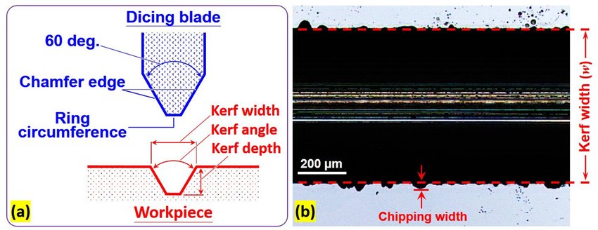
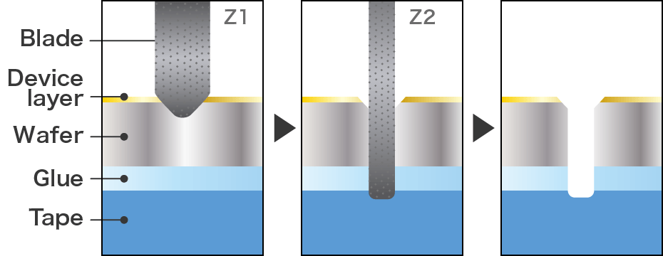
Blade dimensions define the mechanical behavior of the blade during cutting and directly affect kerf loss, precision, and stability.
Blade Thickness
Blade thickness determines structural stiffness and kerf loss. Thinner blades improve die density but reduce stability margin. Thickness selection must consider wafer material and equipment rigidity.
For a detailed engineering analysis, refer to Dicing Saw Blade Thickness.
Blade Width
Blade width defines the effective cutting envelope and governs kerf consistency and blade walking behavior. Width should be minimized while maintaining dynamic stability.
A detailed discussion of width-related precision issues is available in Dicing Saw Blade Width.
Typical Dimension Ranges
| Application | Thickness | Width |
|---|---|---|
| Standard silicon wafers | 20–40 μm | 22–30 μm |
| High-density layouts | 15–25 μm | 20–25 μm |
| SiC / GaN wafers | 40–80 μm | 35–60 μm |
Matching Blades to Wafer Materials
Wafer material properties ultimately define the baseline blade requirements. Silicon wafers allow more flexibility, while compound semiconductors impose stricter constraints.
| Wafer Material | Primary Challenge | Blade Strategy |
|---|---|---|
| Silicon | Chipping control | Thin resin-bond blade |
| SiC | Extreme hardness | Thick metal-bond blade |
| GaN | Microcracking | Moderate grit, stable width |
Material-specific blade requirements are discussed in more detail in Diamond Dicing Blades for Wafers.
Common Dicing Blade Selection Mistakes
Many dicing issues originate from systematic selection errors rather than process tuning mistakes.
Typical Mistakes
- Choosing the thinnest blade without considering stability
- Ignoring equipment torque and runout limitations
- Focusing only on initial kerf width, not kerf consistency
- Using silicon-optimized blades on compound semiconductors
- Skipping pilot validation and edge inspection
These mistakes often result in edge chipping, blade wandering, or unexplained yield loss.
Engineering Checklist Before Final Selection
- Wafer material and thickness confirmed
- Spindle RPM and torque verified
- Flange size and stiffness matched
- Blade thickness and width validated
- Pilot cuts inspected under SEM or optical microscopy
Effective dicing blade selection requires integrating material science, mechanical engineering, and process control. Readers seeking deeper understanding of blade fundamentals should revisit Dicing Blade Technology
By following a structured, engineering-driven selection approach, semiconductor manufacturers can significantly reduce trial-and-error, improve yield stability, and shorten process development cycles.