SiC CMP Polishing Pads for Third-Generation Semiconductors
A complete technical guide to CMP polishing pads for silicon carbide, gallium nitride, and other third-generation semiconductor materials — covering material challenges, pad requirements, slurry compatibility, process recipes, and supplier selection for power device fabs and research labs.
Specialist
- Why SiC Is Different: The Challenge in Numbers
- SiC and GaN Material Properties vs. Silicon
- The Four Core CMP Challenges for SiC
- Pad Requirements: What SiC CMP Demands
- Pad Types Used in SiC CMP
- Slurry-Pad Interaction for SiC
- SiC Wafer Polishing: Three Process Stages
- GaN CMP: Similarities and Differences
- Jizhi SiC Pad Series
- FAQ
Silicon carbide (SiC) and gallium nitride (GaN) are the materials defining the next era of power electronics. SiC-based power MOSFETs and Schottky diodes are displacing silicon IGBTs in electric vehicle (EV) inverters, industrial motor drives, solar inverters, and EV fast-charging stations — enabling systems to operate at higher voltages (600–1700 V), higher temperatures (up to 200°C junction temperature), and higher switching frequencies than silicon can sustain. The global SiC power device market was valued at approximately USD 3.8 billion in 2025 and is projected to exceed USD 12 billion by 2030.
Behind every SiC power device is a substrate polishing process of extraordinary difficulty. SiC’s extreme hardness and chemical inertness make conventional silicon CMP processes nearly useless — achieving the atomically smooth, defect-free surfaces required for epitaxial growth and device fabrication demands specialized CMP polishing pads, purpose-formulated slurries, and optimized process recipes that differ fundamentally from anything used in silicon IC manufacturing.
This guide provides the complete technical picture of SiC CMP polishing pads: what makes SiC so challenging, what properties a pad must have to address those challenges, and how to select and qualify the right pad for your process. For an overview of the broader CMP pad landscape, see: CMP Polishing Pads: The Complete Guide.
1. Why SiC Is Different: The Challenge in Numbers
To appreciate why SiC CMP is so much harder than silicon CMP, it helps to compare the key material properties side by side. The differences are not incremental — they are transformative, requiring an entirely different approach to pad and process design.
The hardness gap between SiC (9.5) and a conventional polyurethane CMP pad (Mohs ~3) is enormous. Standard oxide CMP works because the pad and abrasive (silica, Mohs 7) are harder than the chemically softened SiO₂ surface — the chemistry creates a softer reaction layer that can be mechanically abraded. On SiC, forming an equivalently soft passivation layer requires far more aggressive chemistry, and even then the bulk SiC beneath that layer resists abrasion from any particle softer than itself.
2. SiC and GaN Material Properties vs. Silicon
| Property | Silicon (Si) | 4H-SiC | GaN | CMP Implication |
|---|---|---|---|---|
| Mohs hardness | 6.5 | 9.5 | ~9.0 | Requires diamond or specialty hard abrasives; conventional slurry ineffective |
| Young’s modulus (GPa) | 130–185 | 390–476 | ~295 | Extreme stiffness means brittle fracture rather than plastic deformation during abrasion |
| Chemical inertness | Moderate | Very high | High | Passivation layer forms very slowly; strong oxidizers required at high concentration |
| Thermal conductivity (W/m·K) | 150 | 490 | 230 | High conductivity draws heat away from polishing zone — partially mitigates thermal pad damage |
| Band gap (eV) | 1.12 | 3.26 | 3.39 | Wide bandgap = high device value; surface defect tolerance is much lower than Si |
| Oxidation rate (relative) | 1.0× | ~0.01× | ~0.05× | Chemical passivation rate 20–100× slower than Si; limits achievable MRR with standard chemistry |
3. The Four Core CMP Challenges for SiC
4. Pad Requirements: What SiC CMP Demands from a Polishing Pad
The four challenges above translate directly into pad specification requirements that differ significantly from those for silicon CMP. Understanding these requirements is the foundation of intelligent SiC pad selection.
High Hardness & Wear Resistance
The pad must withstand continuous contact with both SiC (Mohs 9.5) and diamond or boron carbide abrasives in the slurry. Conventional PU pads abrade rapidly under these conditions. Shore D 60–70 with reinforced polymer matrix is the minimum specification. Pad lifetime on SiC is typically 3–5× shorter than on silicon oxide.
Chemical Resistance to Strong Oxidizers
SiC slurries use KMnO₄ (0.5–3 wt%), H₂O₂ (5–30 wt%), or Fenton-type reagents — far more aggressive than the H₂O₂ concentrations used in Cu CMP. The pad polymer must maintain mechanical integrity under these conditions. Polycarbonate-backbone PU or polysiloxane-modified matrices are preferred over standard polyether-PU.
High Thermal Stability (Tg > 110°C)
SiC polishing generates significantly more frictional heat than silicon CMP due to the higher forces required and the lower removal rate (more contact time per unit volume removed). Pad surface temperatures of 70–90°C are common. A glass transition temperature well above 110°C is essential to prevent thermal softening and MRR drift.
Controlled Compliance for Damage Management
For device-layer SiC CMP (final polishing step), the pad must be compliant enough to minimize peak contact stress — reducing the depth of sub-surface damage — while still transmitting sufficient force to maintain acceptable removal rates. This demands precise hardness control in the Shore D 50–60 range for final-step pads.
Groove Design for Aggressive Slurry
Diamond-containing slurries tend to agglomerate under stagnant conditions. Groove design for SiC pads must prioritize slurry refreshment rate and particle resuspension — typically requiring wider, deeper grooves than standard oxide CMP pads, with radial or spiral patterns that maximize centrifugal slurry transport.
Dimensional Stability Under High Down-Force
SiC CMP uses higher down-force pressures than silicon (typically 3–8 psi, versus 1–4 psi for oxide). The pad must maintain its groove geometry and thickness under sustained high load without permanent deformation — requiring high elastic recovery (>80%) and low creep under sustained load.
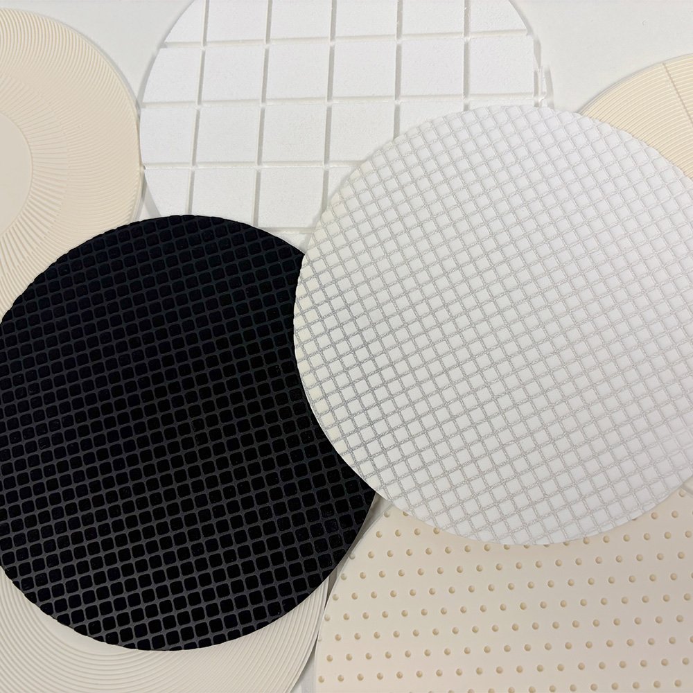
5. Pad Types Used in SiC CMP: A Practical Comparison
Three distinct pad approaches are used in SiC CMP, each making different trade-offs between removal rate, damage depth, and process controllability. The optimal choice depends on which stage of wafer preparation is being performed. For background on pad types in general, see: CMP Pad Materials: Polyurethane vs Other Options.
| Pad Type | MRR on SiC | Sub-Surface Damage | Best Process Stage | Key Limitation |
|---|---|---|---|---|
| Fixed-abrasive diamond pad | 1,000–5,000 Å/min | Deep (200–500 nm) | Coarse lapping / stock removal — not for device-layer CMP | Severe sub-surface damage requires subsequent damage-removal steps |
| Specialty hard PU + diamond slurry | 300–1,200 Å/min | Moderate (50–200 nm) | Intermediate polishing — damage reduction after coarse lapping | Diamond slurry cost; requires strict particle size control to avoid scratch defects |
| Specialty hard PU + oxidizing slurry (ceria/KMnO₄) | 100–600 Å/min | Shallow (<20 nm) | Final CMP — epitaxial-ready surface preparation | Lower MRR demands longer process time; strong oxidizer management required |
| Standard oxide CMP pad (unmodified) | 20–50 Å/min | Minimal | Not commercially viable for SiC production | Insufficient MRR for production throughput regardless of slurry optimization |
6. Slurry-Pad Interaction for SiC: Getting the Chemistry Right
In SiC CMP, the slurry-pad combination is even more tightly coupled than in silicon CMP, because the chemical passivation mechanism is slower and more chemistry-dependent. The pad must be formulated to survive and function efficiently in the aggressive chemical environments that SiC polishing demands.
The SiC Chemical Passivation Mechanism
The most widely used chemical approach to SiC CMP is oxidation-assisted polishing. Strong oxidizing agents convert the SiC surface to a thin (1–3 nm) silicon dioxide (SiO₂) and carbon dioxide layer at the polishing interface. This oxide layer is significantly softer than bulk SiC (Mohs 7 vs. 9.5) and can be removed by the same abrasive particles that would struggle to scratch bulk SiC directly. The overall reaction is approximately:
SiO₂ (soft surface layer) → mechanically removed by abrasive → fresh SiC exposed → cycle repeats
Key Oxidizer Systems and Pad Compatibility
| Oxidizer System | Passivation Rate | MRR Potential | Pad Compatibility | Safety Considerations |
|---|---|---|---|---|
| H₂O₂ (5–30 wt%) | Moderate | 200–500 Å/min | Good with polycarbonate-PU pads | Decomposition produces O₂ — ventilation required |
| KMnO₄ (0.5–3 wt%) | High | 400–800 Å/min | Requires specialty pad — attacks standard PU | Strong oxidizer; MnO₂ byproduct can contaminate wafer |
| Fenton reagent (H₂O₂ + Fe²⁺) | Very high | 500–1,200 Å/min | Attacks most standard PU formulations rapidly | Fe contamination risk; requires careful post-CMP cleaning |
| Electrochemical (anodic oxidation assist) | Controllable | 300–900 Å/min | Compatible with conductive specialty pads | Requires modified tool with electrodes; higher capital cost |
Jizhi Electronic Technology’s SiC pad series uses a polycarbonate-backbone polyurethane matrix with additional cross-linker content, specifically formulated to resist both H₂O₂ (up to 20 wt%) and KMnO₄ (up to 2 wt%) without measurable hardness loss over a 500-wafer pad lifetime. Our material qualification data, including hardness retention after slurry immersion tests at process temperature, is available on request.
7. SiC Wafer Polishing: Three Process Stages and the Right Pad for Each
SiC substrate preparation from an as-sliced ingot to an epitaxial-ready surface is a multi-stage process, each stage requiring a different pad type and process recipe. Understanding the full sequence is essential for specifying the right consumables at each step.
Stage 1 — Coarse Lapping (Stock Removal)
Removes the subsurface damage layer from wire sawing (typically 20–50 µm of damaged crystal must be removed). Uses diamond lapping plates or coarse fixed-abrasive pads with 6–15 µm diamond abrasive. Removal rate: 2,000–10,000 Å/min. Surface after this stage: Ra 50–200 nm, sub-surface damage depth 0.5–2 µm. A conventional CMP pad is not used at this stage — this is pure mechanical lapping.
Stage 2 — Damage Removal CMP (Intermediate Polish)
The critical transition step. Uses a specialty hard PU pad (Shore D 62–68, polycarbonate-backbone) with a diamond slurry (0.1–0.5 µm diamond, pH 8–10, H₂O₂ 5–15 wt%). Target: removal of 5–15 µm of material, reducing Ra from 50–200 nm to 1–5 nm, and reducing sub-surface damage depth from 0.5–2 µm to <30 nm. Removal rate: 300–800 Å/min. Down-force: 4–8 psi. This is where Jizhi’s JZ-SiC-I series pad is designed to operate.
Stage 3 — Final CMP (Epitaxial-Ready Surface)
The highest-precision step. Uses a medium-hard specialty PU pad (Shore D 52–60, controlled compliance) with colloidal ceria or fine silica slurry (pH 9–11, KMnO₄ 0.5–1.5 wt% or H₂O₂ 10–20 wt%). Target: Ra < 0.2 nm, sub-surface damage depth <5 nm, surface step density <0.1 steps/µm². Removal rate: 80–300 Å/min. Down-force: 1.5–3 psi. This step is the most critical determinant of epilayer quality and device performance. Jizhi’s JZ-SiC-II series is engineered for this stage.
8. GaN CMP: How It Differs from SiC
Gallium nitride presents a related but distinct CMP challenge from SiC. GaN is used primarily in RF power amplifiers (for 5G base stations), high-electron-mobility transistors (HEMTs), and, increasingly, in GaN-on-Si power switches competing with SiC in the 600 V range.
🔴 Where GaN CMP Is Harder Than SiC
- GaN is chemically even more inert than SiC under most oxidizing conditions — its Ga-N bond energy (8.92 eV/bond) is very high
- Effective wet chemical etchants for GaN are limited to hot KOH (anisotropic) — not usable in CMP
- GaN is typically grown as a thin epilayer on Si, SiC, or sapphire substrates — polishing through the GaN without damaging the substrate or the active device region below requires exceptional endpoint control
- Polarity matters: N-face GaN polishes at a dramatically different rate than Ga-face GaN, creating non-uniformity risk on wafers with any polarity domains
🟢 Where GaN CMP Is More Tractable Than SiC
- GaN-on-Si substrates benefit from the relative ease of polishing Si — the GaN layer CMP can use the Si substrate as a natural stop layer
- Photo-enhanced CMP (using UV illumination to generate photo-carriers that accelerate oxidation) is particularly effective on GaN, enabling higher MRR without requiring extreme oxidizer concentrations
- For GaN power devices, the CMP requirements are often less stringent than for SiC epitaxial substrates — Ra < 1 nm is typically acceptable rather than < 0.2 nm
- Pad requirements are similar to Stage 3 SiC CMP — medium-hard specialty PU with high chemical resistance
9. Jizhi SiC CMP Pad Series
Jizhi Electronic Technology has developed a dedicated SiC CMP pad series through a multi-year R&D program combining polymer materials science, tribology characterization, and SiC process engineering. Our pads are actively supplied to power device fabs, SiC substrate manufacturers, and university research groups as of April 2026.
| Product | Shore D | Polymer Matrix | Target Stage | Compatible Slurry | Typical MRR |
|---|---|---|---|---|---|
| JZ-SiC-I | 63–68 | Polycarbonate-PU, high cross-link density | Stage 2 — damage removal | Diamond 0.1–0.5 µm + H₂O₂ 10–20% | 350–800 Å/min |
| JZ-SiC-II | 53–60 | Polycarbonate-PU, controlled compliance | Stage 3 — final CMP | Ceria or silica + KMnO₄ 0.5–1.5% or H₂O₂ 10–20% | 100–350 Å/min |
| JZ-GaN-F | 50–58 | Polycarbonate-PU, UV-transparent variant | GaN final CMP | Colloidal silica + mild oxidizer, pH 9–11 | 80–250 Å/min |
| JZ-SiC-Custom | Customer-specified | Per application requirement | Custom process step | Validated per customer slurry | Per characterization |
For customers requiring custom pad formulations — for example, for 200 mm SiC wafers, Ga₂O₃ substrates, diamond substrates, or proprietary slurry systems — Jizhi’s application engineering team manages the full co-development cycle. See our custom pad development program at: Custom CMP Polishing Pad Solutions.