The “Surface Revolution” in Semiconductor Manufacturing: The Technical Essence and Foundational Value of Silicon Wafer Polishing
In the precision manufacturing chain of the semiconductor industry, the creation of every high-performance chip relies on hundreds of process steps, from silicon purification to chip packaging. Among these, silicon wafer polishing—a critical process connecting wafer cutting and grinding with subsequent lithography and thin-film deposition—can be called the “art of surface finishing” in semiconductor manufacturing. It shapes the wafer surface with nanometer-level precision, directly determining the chip’s performance, reliability, and yield. As a company deeply rooted in the electronics field, Gizhi Electronics fully understands the core value of this process. This article will delve into the technical essence of silicon wafer polishing.
Why is Silicon Wafer Polishing a “Required Task” in Semiconductor Manufacturing?
After processes like cutting and grinding, the wafer surface retains micron-level damage layers, scratches, uneven rough structures, and may also have attached impurity particles. If not addressed promptly, these defects can directly lead to distorted lithography patterns, uneven thin-film deposition, and even fatal issues such as device leakage or breakdown. Therefore, the core goal of silicon wafer polishing is not simply to “make it smooth” but to achieve three key objectives through precise control:
-
Eliminate Surface Damage and Restore Micro-Level Flatness: Completely remove lattice damage layers and mechanical scratches generated in previous processes, reducing wafer surface roughness to the nanometer or even sub-nanometer level, ensuring highly uniform surface microtopography.
-
Ensure Dimensional Accuracy and Achieve Global Consistency: Strictly control wafer thickness deviation and flatness to meet the stringent requirements of lithography processes for a “reference plane,” avoiding exposure errors caused by local thickness variations.
-
Purify the Surface Environment and Enhance Device Reliability: Through physical friction and chemical reactions during polishing, remove adsorbed impurity ions and micro-particles from the surface, reducing defect sources during device fabrication, and improving chip lifespan and stability from the source.
Mainstream Technology: The “Synergistic Magic” of Chemical Mechanical Polishing (CMP)
Currently, over 90% of silicon wafer polishing tasks in semiconductor manufacturing are handled by Chemical Mechanical Polishing (CMP) technology. The core advantage of this technology lies in maximizing the synergistic effects of “chemical corrosion” and “mechanical grinding.” It avoids surface damage caused by purely mechanical grinding while addressing the difficulty of controlling flatness with purely chemical corrosion. The core logic of its process can be summarized as the precise matching of three key elements:
-
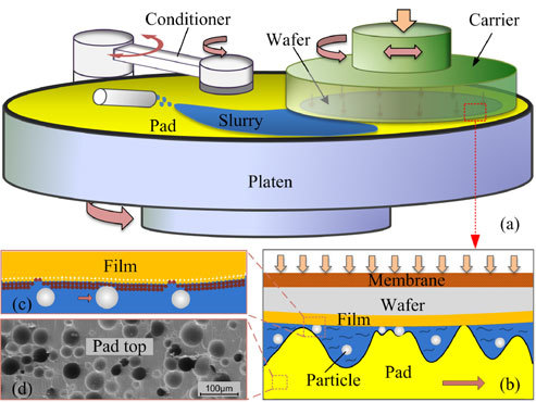
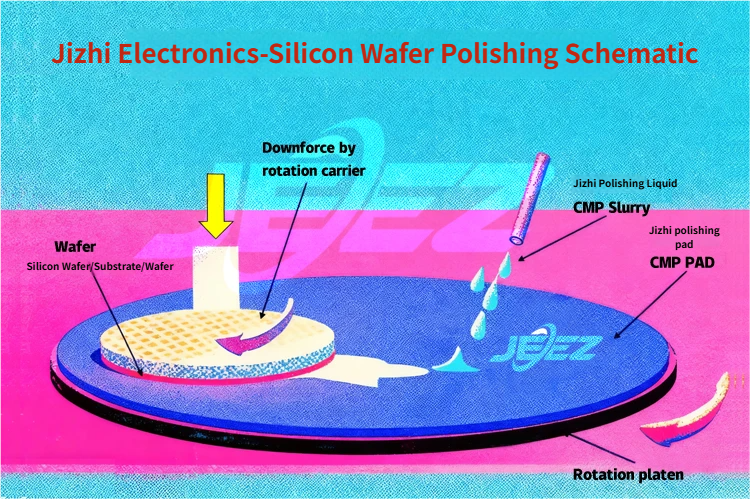
Core Consumables: The “Golden Partnership” of Polishing Slurry and Polishing Pad
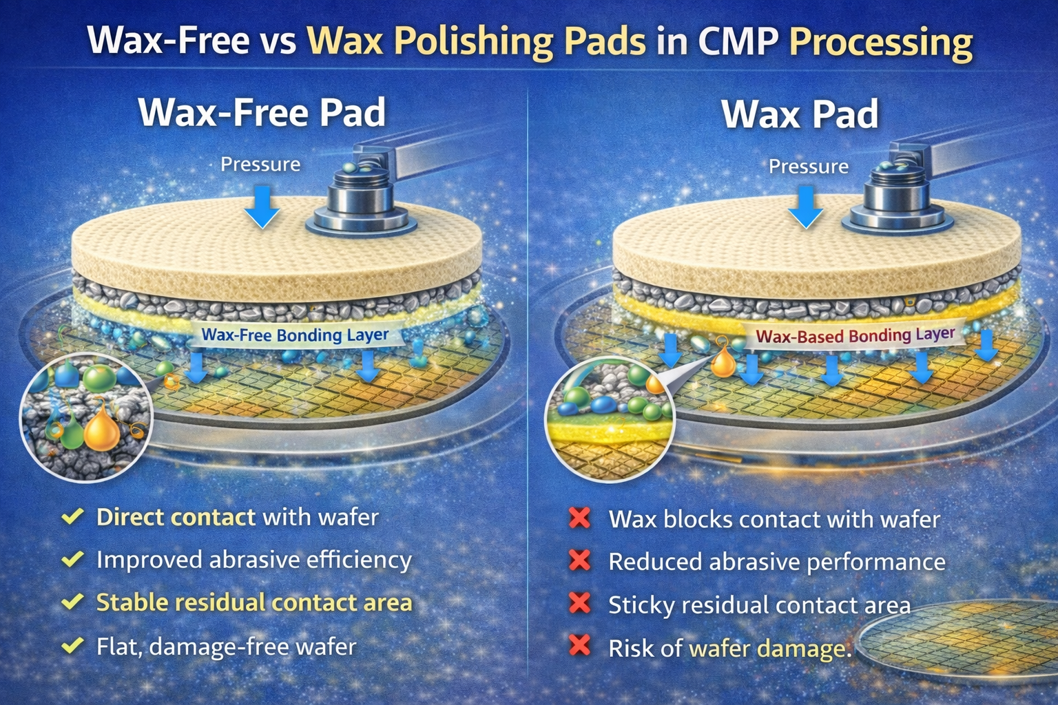
Polishing slurry is the “chemical core” of CMP, typically formulated with abrasive particles (e.g., silicon dioxide, aluminum oxide), chemical etchants (e.g., potassium hydroxide, hydrogen peroxide), stabilizers, and other components. Among these, abrasive particles provide the “cutting force” for mechanical grinding, while chemical etchants oxidize silicon atoms on the wafer surface into a removable oxide layer. The combination of these two enables efficient and low-damage material removal. The polishing pad, as the “force-bearing carrier,” not only transmits grinding pressure but also removes waste and heat generated during polishing through its porous structure, maintaining polishing environment stability. The application of adsorption pad technology further enhances the efficiency and yield of wafer polishing. -
Process Control: The “Precision Game” of Pressure, Speed, and Time
During CMP, the wafer is adsorbed under the polishing head and pressed against the rotating polishing pad at a specific speed while polishing slurry is continuously and evenly sprayed at the interface. Polishing pressure directly determines the material removal rate, the speed ratio affects polishing uniformity, and polishing time precisely controls the final wafer thickness. For large-sized 12-inch wafers, the control precision of these parameters must reach millisecond and micrometer levels, as any slight deviation could render an entire batch of wafers unusable. -
Post-Process Assurance: The “Dual Check” of Cleaning and Inspection
After polishing, residual particles and chemical impurities from the polishing slurry remain on the wafer surface and must be completely removed through multi-step cleaning processes (e.g., ultrasonic cleaning). The cleaned wafers then undergo rigorous quality inspection: surface roughness is measured using Atomic Force Microscopy (AFM), flatness is assessed via laser interferometry, and surface impurities are checked with particle counters. Only wafers meeting all semiconductor-grade standards can proceed to subsequent lithography processes.
Technological Evolution: The “Precision Race” Keeping Pace with Chip Process Advancement
As chip processes advance from micrometer levels to 7nm, 5nm, and even more advanced nodes, the technical requirements for silicon wafer polishing continue to break new ground. For example, wafers used in 3D NAND flash memory require not only higher surface flatness but also “global planarization” to adapt to multi-layer stacking structures. For thick wafers used in power semiconductors, polishing must balance thickness uniformity with mechanical strength. To address these challenges, polishing technology is evolving toward “consumable customization” and “process intelligence,” using AI algorithms to adjust polishing parameters in real time and combining customized polishing slurry formulations to meet the personalized needs of different chip scenarios.