Wafer Dicing Blades for Semiconductor Applications
Wafer dicing blades are precision cutting tools used in semiconductor manufacturing to separate processed wafers into individual dies. Although dicing is one of the final steps in wafer fabrication, its impact on overall device yield, reliability, and downstream assembly quality is significant. As device dimensions shrink and wafer materials diversify, dicing blades are required to operate within increasingly narrow process windows while maintaining high cutting accuracy and stability.
Unlike conventional cutting tools, wafer dicing blades operate at micrometer-scale tolerances and must remove brittle materials under high spindle speeds without inducing excessive chipping, micro-cracks, or subsurface damage. In production environments, blade performance directly affects kerf loss, edge quality, die strength, and ultimately the cost per good die. For this reason, wafer dicing blades are not consumables selected solely on price, but engineered tools that must be matched carefully to wafer materials, equipment, and process objectives.
This page provides a technically oriented overview of wafer dicing blades used in semiconductor applications. It explains blade types, diamond blade construction principles, critical parameters influencing cutting performance, and engineering considerations for blade selection. The goal is to provide clear, practical guidance that supports both process optimization and sourcing decisions.
Table of Contents
- What Are Wafer Dicing Blades?
- Types of Dicing Blades Used in Semiconductor Manufacturing
- Diamond Dicing Blades for Precision Wafer Cutting
- Key Parameters of Dicing Saw Blades
- Applications of Wafer Dicing Blades
- How to Choose the Right Dicing Blade
- Wafer Dicing Blade Supplier & Custom Solutions
What Are Wafer Dicing Blades?
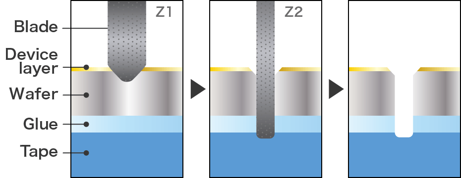
Wafer dicing blades are ultra-thin circular saw blades mounted on high-speed spindles in dicing saw machines. Their primary function is to cut along predefined scribe lines on a wafer, separating it into individual semiconductor dies with minimal material loss and mechanical damage. Typical blade thickness ranges from tens to a few hundreds of micrometers, while operating speeds often exceed 20,000–40,000 rpm.
During the dicing process, the wafer is supported on adhesive dicing tape and held flat by a vacuum chuck. The rotating blade engages the wafer material under controlled feed rates and cutting depths. Because semiconductor wafers are brittle and often contain multiple layers with different mechanical properties, the cutting process must be highly stable. Any fluctuation in blade condition or cutting parameters can result in edge chipping, delamination, or latent cracks that may not be detected until later reliability testing.
As wafer diameters increase and device layouts become denser, the tolerance for dicing-related defects continues to decrease. This has driven continuous development in dicing blade technology, focusing on blade materials, bonding systems, and structural optimization to improve cutting consistency and tool life.
Types of Dicing Blades Used in Semiconductor Manufacturing
Dicing blades used in semiconductor manufacturing can be categorized based on abrasive material and bonding method. While early-generation blades relied on conventional abrasives, modern semiconductor processes overwhelmingly use diamond-based blades due to their superior hardness and wear resistance.
Non-diamond abrasive blades, such as silicon carbide or aluminum oxide blades, are occasionally used for low-hardness substrates or non-critical applications. However, their limited durability and inconsistent cutting behavior make them unsuitable for advanced semiconductor wafers where edge integrity and dimensional control are critical.
Diamond dicing blades represent the industry standard for wafer cutting. Synthetic diamond abrasives provide the necessary hardness to cut silicon, glass, sapphire, and compound semiconductors while maintaining stable cutting geometry over extended production runs. The performance of these blades is governed not only by diamond hardness but also by the bonding system that holds the diamond particles in place.
Different bonding technologies—such as resin bond, metal bond, and electroformed bond—result in distinct cutting characteristics. These differences are discussed in detail in our dedicated overview of dicing blade technology in semiconductor manufacturing.
Diamond Dicing Blades for Precision Wafer Cutting
Diamond dicing blades are engineered composites consisting of diamond abrasive particles embedded in a bonding matrix. During cutting, diamond grains perform the material removal, while the bond controls grain retention, exposure rate, and blade wear behavior. The interaction between diamond and bond determines cutting aggressiveness, surface finish, and blade lifespan.
For precision wafer cutting, diamond dicing blades must achieve a balance between sharpness and stability. Excessively aggressive blades may increase cutting speed but can introduce chipping and subsurface damage. Conversely, overly soft or fine-grit blades may produce excellent edge quality at the expense of throughput and frequent blade replacement.
Advanced diamond blade designs optimize grain size distribution, diamond concentration, and bond formulation to match specific wafer materials and thicknesses. These design principles are explored further in our product-focused guide on Diamond Dicing Blades and application-specific page on Diamond Dicing Blades for Wafers.
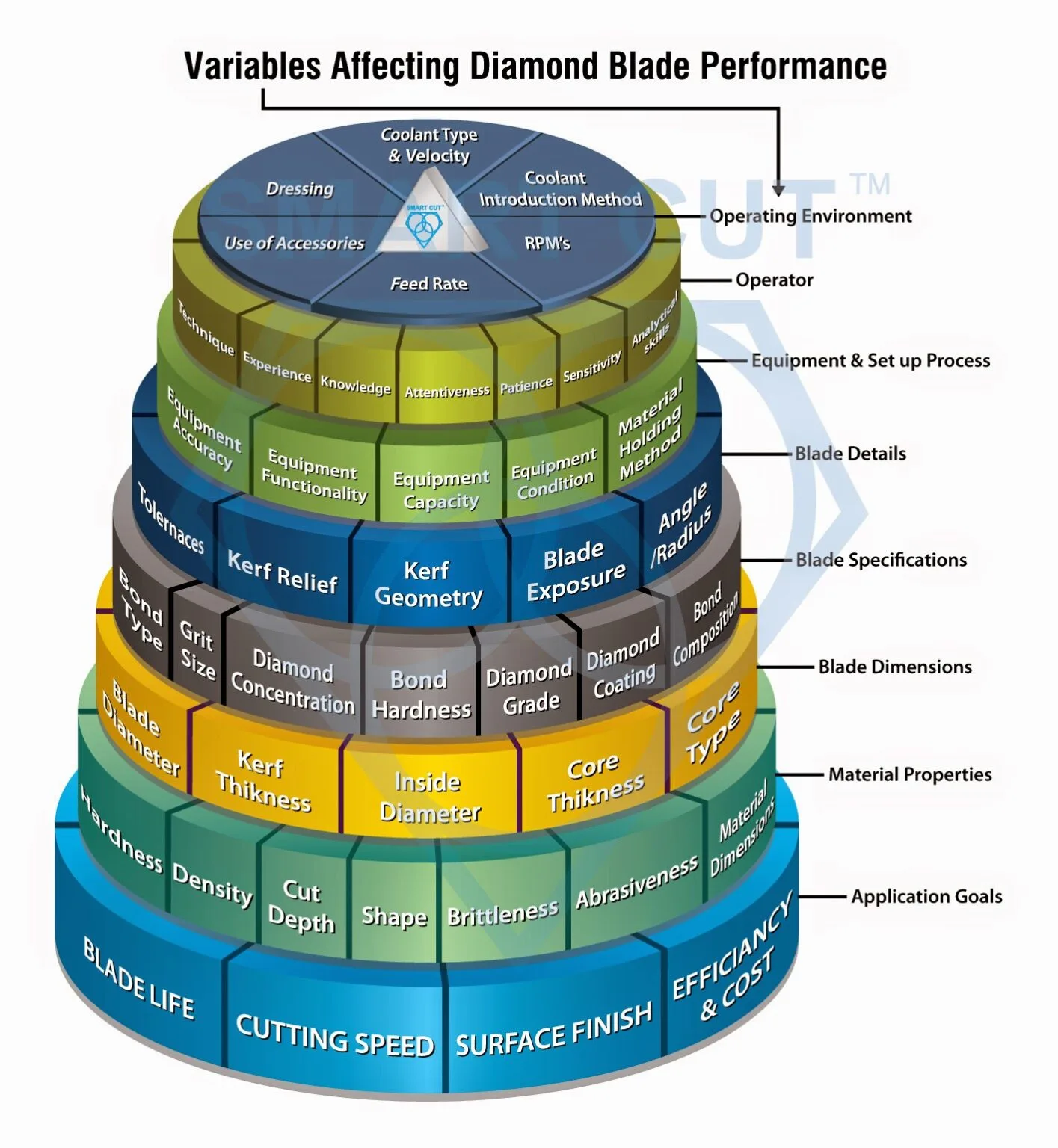
Key Parameters of Dicing Saw Blades
Several blade parameters directly influence dicing performance and must be considered together rather than in isolation. Key parameters include blade thickness, blade width, grit size, diamond concentration, and bond type. Improper optimization of any one parameter can compromise overall process stability.
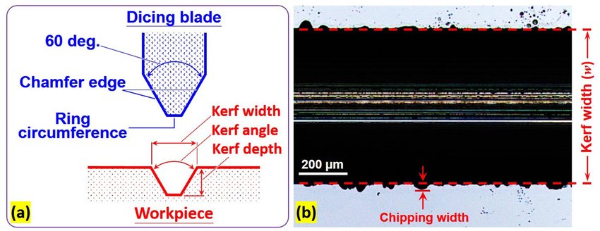
Blade thickness affects both kerf loss and mechanical rigidity. Thinner blades reduce material loss and increase die count per wafer, but they are more susceptible to deflection and vibration. A detailed engineering discussion of this trade-off is provided in our guide on dicing saw blade thickness.
Blade width determines the effective kerf width and directly influences scribe line design and die spacing. Kerf control becomes increasingly critical as device layouts shrink. Optimization strategies are discussed in our article on dicing saw blade width and kerf control.
Grit size and diamond concentration influence cutting smoothness, blade wear rate, and thermal behavior. Standardized definitions and customization options are summarized in Dicing Blade Specifications Explained.
Applications of Wafer Dicing Blades
Wafer dicing blades are used across a broad range of semiconductor applications, including logic ICs, memory devices, power semiconductors, MEMS, sensors, LEDs, and compound semiconductor devices. Each application presents unique challenges related to wafer hardness, thickness, and sensitivity to mechanical stress.
For example, silicon wafers used in logic and memory devices prioritize kerf control and throughput, while compound semiconductors such as SiC and GaAs require enhanced blade durability and edge integrity. Equipment compatibility and setup considerations are discussed in our overview of wafer dicing blades and dicing equipment.
How to Choose the Right Dicing Blade
Selecting the right dicing blade requires a systematic evaluation of wafer material, device structure, equipment limitations, and production targets. There is no universal blade suitable for all applications; optimal selection is always application-specific.
Key selection factors include wafer thickness, required kerf width, acceptable edge damage levels, spindle capability, and expected production volume. Common selection mistakes—such as prioritizing blade life over edge quality or ignoring equipment constraints—can lead to yield loss and higher overall cost.
A structured, engineering-based selection methodology is provided in our high-intent guide on how to choose dicing blades.
Wafer Dicing Blade Supplier & Custom Solutions
As semiconductor processes continue to diversify, standard catalog blades are often insufficient. Custom dicing blade solutions allow fine-tuning of bond composition, diamond characteristics, and blade geometry to meet specific process requirements.
A capable wafer dicing blade supplier should provide not only products, but also application support, process testing, and consistent quality control. In high-volume manufacturing, the right blade partner can reduce total cost of ownership by improving yield stability, extending blade life, and minimizing rework caused by dicing-related defects.
For further technical insight, continue with our in-depth discussion on Dicing Blade Technology in Semiconductor Manufacturing, which serves as the first cluster page supporting this pillar.