Wax-Free Adsorption Polishing Pad Technology
Table of Contents
- 1. Technology Overview: Adsorption as a Replacement for Wax Bonding
- 2. Fundamental Sources of Adsorption Force in Wax-Free Pads
- 3. Pad Microstructure Design and Adsorption Efficiency
- 4. Contact Mechanics at the Pad–Wafer Interface
- 5. Tunable Engineering Parameters Affecting Adsorption
- 6. Adsorption Stability Under CMP Operating Conditions
- 7. Adsorption Degradation and Failure Modes
- 8. Position of Adsorption Technology Within CMP Systems
1. Technology Overview: Adsorption as a Replacement for Wax Bonding
Wax-free adsorption polishing pad technology was developed to eliminate the inherent limitations of wax-based wafer bonding in CMP. Traditional wax layers introduce viscoelastic behavior, thermal sensitivity, thickness variability, and chemical interaction with slurry components. Adsorption-based systems replace these variables with mechanically governed interface control.
In wax-free pads, wafer holding force is generated through pressure-induced conformity, interface sealing, and frictional resistance rather than chemical adhesion. This shift fundamentally changes how holding force responds to load, temperature, and motion, making adsorption technology inherently more predictable and scalable for advanced semiconductor manufacturing.
2. Fundamental Sources of Adsorption Force in Wax-Free Pads
Adsorption force in wax-free polishing pads is not derived from a single physical phenomenon but from the combined effect of multiple mechanical contributors. These contributors act simultaneously at the pad–wafer interface and scale dynamically with applied pressure.
The primary contributors to adsorption force include interfacial pressure sealing, elastic deformation-induced conformity, and frictional resistance to lateral motion. Unlike vacuum chucks, wax-free pads do not require external pressure differentials; adsorption emerges naturally from mechanical contact conditions.
| Adsorption Contributor | Engineering Description |
|---|---|
| Pressure sealing | Reduction of interfacial air volume under load |
| Elastic conformity | Increased real contact area through deformation |
| Frictional resistance | Lateral force suppression during rotation |
3. Pad Microstructure Design and Adsorption Efficiency
Pad microstructure plays a decisive role in determining adsorption efficiency. Surface asperity geometry, pore size distribution, and pore connectivity collectively influence how air is displaced, how pressure is transmitted, and how contact area evolves under load.
Pads designed for wax-free adsorption typically employ controlled micro-porosity to balance air evacuation and structural integrity. Excessively open structures reduce sealing efficiency, while overly dense structures inhibit deformation and adsorption development.
| Microstructural Feature | Functional Impact |
|---|---|
| Surface roughness | Controls initial contact and air escape |
| Pore size | Balances evacuation and load support |
| Pore connectivity | Enables uniform pressure distribution |
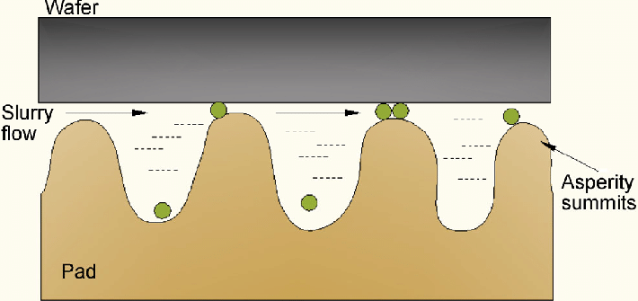
4. Contact Mechanics at the Pad–Wafer Interface
From a contact mechanics perspective, wax-free adsorption pads operate in a regime where elastic deformation dominates over plastic flow. The pad material must be compliant enough to conform to wafer backside topography while maintaining sufficient stiffness to transmit polishing pressure uniformly.
As load increases, the real contact area grows nonlinearly, enhancing both adsorption force and frictional stability. This behavior allows adsorption strength to self-adjust in response to process conditions, a feature absent in wax-based bonding systems.
5. Tunable Engineering Parameters Affecting Adsorption
One of the major advantages of wax-free adsorption technology is its tunability. Adsorption behavior can be engineered through material formulation and structural design without altering CMP tool hardware.
| Parameter | Typical Range | Effect on Adsorption |
|---|---|---|
| Elastic modulus | 10–50 MPa | Controls deformation and contact growth |
| Pad thickness | 1.0–3.0 mm | Affects pressure distribution |
| Surface roughness (Ra) | 3–10 μm | Influences initial sealing |
| Porosity | 20–50% | Balances sealing and compliance |
6. Adsorption Stability Under CMP Operating Conditions
During CMP, adsorption technology must remain stable under combined mechanical, thermal, and chemical stress. Wax-free adsorption pads exhibit stable behavior across typical CMP operating temperatures because no thermally sensitive bonding layer is present.
Additionally, because adsorption force scales with applied pressure, transient fluctuations in load or speed do not result in sudden loss of wafer holding, contributing to improved process robustness.
7. Adsorption Degradation and Failure Modes
Although wax-free adsorption technology eliminates many wax-related risks, adsorption performance can degrade if pad surface condition, pore structure, or elastic properties drift outside design limits. Common degradation mechanisms include surface glazing, pore clogging, and excessive wear.
Understanding these failure modes allows preventive maintenance strategies to be implemented without introducing additional process complexity.
| Failure Mode | Underlying Cause |
|---|---|
| Reduced adsorption | Surface smoothing or pore blockage |
| Non-uniform holding | Localized modulus variation |
| Premature release | Excessive pad wear |
8. Position of Adsorption Technology Within CMP Systems
Wax-free adsorption polishing pad technology functions as a foundational element within the broader CMP system architecture. It directly influences wafer stability, pressure transfer, and process repeatability, while enabling simplified integration with advanced CMP recipes.
For a process-sequenced explanation of how adsorption behavior evolves during CMP operation, refer to How Wax-Free Polishing Pads Work. For a system-level overview and navigation to related topics, to page Wax-Free CMP Polishing Pads.