What Is CMP Slurry? A Complete Guide to Chemical Mechanical Planarization Slurry
From wafer-level planarization at the 3nm node to advanced packaging for chiplets, CMP slurry is the consumable that makes modern semiconductor manufacturing possible. This guide covers everything you need to know — chemistry, process, types, suppliers, and market trends.
📋 Table of Contents
- What Is CMP Slurry?
- How the CMP Process Works
- CMP Slurry Composition: The Three Pillars
- Types of CMP Slurry
- Key Performance Metrics
- CMP Slurry vs. CMP Pad
- CMP Slurry for Advanced Nodes (5nm, 3nm & Beyond)
- Top CMP Slurry Manufacturers
- Market Outlook & Industry Trends
- How to Select the Right CMP Slurry
- Quality Control & Defect Management
- Frequently Asked Questions
1. What Is CMP Slurry?
CMP slurry — short for Chemical Mechanical Planarization slurry — is a precisely engineered liquid abrasive used in semiconductor manufacturing to polish and flatten the surface of silicon wafers and thin-film layers. It is the consumable medium through which the CMP process simultaneously removes material chemically and mechanically, achieving nanometer-scale surface uniformity that no other technique can match.
First commercialized by IBM in the late 1980s for oxide planarization on CMOS logic devices, CMP slurry has evolved into one of the most complex and critically specified consumables in the entire semiconductor supply chain. Today, a leading-edge fab running at 3nm may apply CMP slurry across 20 or more distinct process steps — each requiring a different slurry formulation tailored to the target film, removal rate, and defectivity budget.
📌 Quick Definition
CMP slurry is an aqueous suspension of abrasive nanoparticles combined with chemical agents (oxidizers, chelators, inhibitors, pH buffers, and surfactants) that together enable the controlled removal and planarization of dielectric, metal, or barrier films on a semiconductor wafer surface during the CMP process.
Unlike bulk polishing compounds used in optics or metallurgy, semiconductor-grade CMP slurry must maintain extraordinary particle size distribution control (often ±5 nm from the mean), extremely low levels of metal ion contamination (<1 ppb), and batch-to-batch chemical repeatability measured to parts per million. These requirements make CMP slurry one of the most technically demanding specialty chemicals in industrial production.
2. How the CMP Process Works
To understand the role of CMP slurry, it helps to understand the CMP process as a whole. Chemical mechanical planarization is a wafer-finishing technique that combines two distinct material-removal mechanisms — chemical reactions and mechanical abrasion — working simultaneously to produce a globally flat, highly polished surface.
-
1
Wafer Mounting & Pressure Application The wafer is held face-down in a carrier head and pressed against a rotating polishing pad (typically polyurethane) mounted on a rotating platen. Downforce (typically 1–6 psi) is applied uniformly across the wafer surface.
-
2
Slurry Delivery CMP slurry is continuously dispensed onto the polishing pad — typically at flow rates of 100–300 mL/min — and distributed across the pad surface through the relative motion of pad and wafer. Slurry delivery uniformity is a major process control variable.
-
3
Chemical Softening The chemical agents in the slurry react with the wafer surface film to form a softer reaction layer. For example, in copper CMP, oxidizers such as hydrogen peroxide convert the Cu surface to Cu(OH)₂ or CuO, which is mechanically weaker than the base metal.
-
4
Mechanical Abrasion Abrasive nanoparticles suspended in the slurry — silica, ceria, or alumina — physically remove the chemically softened surface material as they pass between the wafer and the pad. The combined synergy produces material removal rates (MRR) far higher than either mechanism alone.
-
5
Byproduct Removal & Post-CMP Clean Material removed from the wafer is carried away in the slurry effluent. After polishing, the wafer undergoes post-CMP cleaning (brush scrub + dilute chemical clean) to remove residual abrasive particles and reaction byproducts. Slurry particle adhesion force and surface chemistry strongly influence cleaning efficiency.
⚙️ Preston’s Equation — The CMP Governing Formula
Material removal rate (MRR) in CMP is approximated by Preston’s equation: MRR = Kp × P × V, where Kp is the Preston coefficient (a material-dependent constant), P is applied pressure, and V is the relative velocity between wafer and pad. Slurry chemistry modifies Kp, making it the primary lever for tuning selectivity and removal rate without changing tool hardware.
3. CMP Slurry Composition: The Three Pillars
Every CMP slurry formulation — regardless of application — is built on three foundational components. Understanding their roles is essential for process engineers evaluating or qualifying a new slurry. For a deeper technical breakdown, see our dedicated guide on CMP Slurry Composition: Abrasives, Chemicals & Formulation.
3.1 Abrasive Particles
The abrasive component provides mechanical cutting action. The three most commercially important abrasive materials are:
| Abrasive Type | Particle Size Range | Mohs Hardness | Primary Applications | Key Advantage |
|---|---|---|---|---|
| Colloidal Silica (SiO₂) | 10–150 nm | 6–7 | Oxide ILD, Poly-Si, Final polish | Low defectivity, high purity |
| Cerium Oxide (CeO₂) | 20–300 nm | 6 | STI, FEOL oxide, Low-k dielectric | Extremely high oxide selectivity vs. nitride |
| Alumina (Al₂O₃) | 50–500 nm | 9 | Tungsten plug, Hard metals, Sapphire | High MRR on hard materials |
Abrasive concentration in slurry typically ranges from 1 wt% to 12 wt%. Higher concentrations generally increase MRR but also raise the risk of scratching and wafer-level defects. Abrasive particle shape (spherical vs. irregular), surface chemistry (surface OH density), and colloidal stability (characterized by zeta potential) are equally critical parameters.
3.2 Chemical Agents
The chemical package in CMP slurry can contain six or more distinct additive classes, each performing a specific function:
- Oxidizers (H₂O₂, KIO₃, Fe(NO₃)₃): Convert metal surfaces to softer oxide or hydroxide layers, enabling mechanical removal. H₂O₂ dominates in copper CMP; iodate-based oxidizers are used in some tungsten slurries.
- Complexing/Chelating Agents (citric acid, amino acids, BTA): Chelate dissolved metal ions to prevent re-deposition and control corrosion. Benzotriazole (BTA) is widely used as a copper corrosion inhibitor in Cu CMP.
- pH Buffers & Regulators: Most slurries operate at tightly controlled pH ranges — acidic (pH 2–4) for metal CMP, alkaline (pH 9–12) for oxide slurries. Even small pH excursions can collapse abrasive dispersion stability.
- Surfactants & Dispersants: Prevent particle agglomeration, modify the slurry-pad interface, and influence the fluid film thickness between wafer and pad.
- Inhibitors: Protect already-planarized recessed areas from continued removal (e.g., dishing control in metal CMP).
- Biocides: Prevent microbial growth during storage and distribution, which can alter slurry pH and cause particle flocculation.
3.3 Deionized Water (DIW) Carrier
Ultrapure deionized water serves as the slurry carrier medium, typically comprising 85–95% of total slurry volume. The DIW must meet SEMI grade specifications — typically resistivity >17.5 MΩ·cm and total organic carbon (TOC) <5 ppb — to prevent ionic contamination of the slurry chemistry or the wafer surface.
4. Types of CMP Slurry
CMP slurry is not a single product — it is a broad family of formulations differentiated by target film, process node, and performance requirements. Our comprehensive breakdown is available in the dedicated article on CMP Slurry Types: Oxide, Metal, STI & Beyond. The primary categories are summarized here:
4.1 Oxide CMP Slurry (ILD)
Oxide slurry is used to planarize inter-layer dielectric (ILD) films, primarily TEOS-based SiO₂ deposited by PECVD or HDP-CVD. It is typically alkaline (pH 10–11), silica-abrasive based, and achieves oxide MRR of 1,000–3,000 Å/min. Oxide CMP was historically the first CMP application and remains the highest-volume slurry segment by wafer area.
4.2 STI (Shallow Trench Isolation) Slurry
STI slurry must remove TEOS oxide while stopping precisely on a silicon nitride (Si₃N₄) stop layer — a selectivity ratio of 100:1 or higher is routinely demanded at advanced nodes. Ceria-based abrasives with anionic polymer additives are the state of the art for achieving this high SiO₂:Si₃N₄ selectivity, critical in FEOL transistor isolation. This is also the main application driving the adoption of ceria abrasive technology.
4.3 Copper CMP Slurry
Copper dual damascene interconnect fabrication requires a multi-step CMP sequence: bulk copper removal (step 1), barrier/liner removal (step 2), and optional dielectric buff (step 3). Each step uses a different slurry optimized for the target film. The bulk Cu slurry is highly selective (Cu:barrier >100:1), while the barrier slurry achieves near-unity selectivity across Cu, Ta/TaN, and SiO₂. Our in-depth article on Copper CMP Slurry covers formulation principles and process integration in detail.
4.4 Tungsten CMP Slurry
Tungsten plug and contact CMP uses highly acidic slurry (pH 2–4) with iron nitrate or iodate oxidizers and alumina abrasives to remove W at rates of 2,000–5,000 Å/min while stopping on a Ti/TiN barrier. Tungsten slurry management is particularly demanding due to the corrosive chemistry and abrasive hardness involved in wafer handling and slurry waste treatment.
4.5 Barrier / Liner CMP Slurry
Barrier slurry removes tantalum nitride (TaN) and tantalum (Ta) barrier layers after bulk copper CMP with controlled selectivity across Cu, Ta, and dielectric. Achieving low dishing and erosion in this step is critical to resistance uniformity in interconnect lines, particularly in advanced BEOL layers below 28nm.
4.6 Polysilicon CMP Slurry
Used in FEOL gate and DRAM cell fabrication, polysilicon CMP slurry is typically silica-based with high poly:oxide selectivity (>50:1) to accurately stop on gate oxide layers without damaging the underlying dielectric.
5. Key Performance Metrics for CMP Slurry Evaluation
When qualifying a CMP slurry for production, process engineers evaluate performance across five core dimensions. Understanding these metrics is equally essential for procurement teams specifying slurry requirements from suppliers.
| Metric | Definition | Typical Target | Impact of Non-Compliance |
|---|---|---|---|
| Material Removal Rate (MRR) | Thickness of film removed per unit time (Å/min) | 500–5,000 Å/min (application-dependent) | Under-polish or over-polish; throughput loss |
| Selectivity | Ratio of MRR of target film to stop-layer film | 10:1 to 100:1 (STI: >100:1) | Loss of process window; stop-layer consumption |
| Within-Wafer Non-Uniformity (WIWNU) | Variation in remaining film thickness across wafer (%) | <3% (1σ); <1.5% at advanced nodes | Parametric yield loss; resistance variation |
| Defectivity | Surface defects per wafer post-CMP (scratches, pits, particles) | <50 defects/wafer at 300mm; critical defects <5 | Device failure; yield fallout; reliability risk |
| Dishing & Erosion | Over-removal of metal center (dishing) or of array areas (erosion) | <30 nm dishing; <20 nm erosion at <10nm node | RC delay increase; reliability failure in interconnects |
These metrics are interdependent — formulation changes that boost MRR often increase defectivity or worsen selectivity. The role of a CMP slurry supplier is to deliver a formulation that simultaneously optimizes all five metrics within the process window of the customer’s specific CMP tool, pad type, and integration scheme. For a detailed discussion of defect control, see our guide on CMP Slurry Defects Analysis & Quality Control.
6. CMP Slurry vs. CMP Pad: Understanding the Relationship
CMP slurry and the CMP polishing pad are the two primary consumables in every CMP process, and their performance is deeply intertwined. Neither can be optimized in isolation. A full comparison of these two consumables is available in CMP Slurry vs. CMP Pad: Differences & Synergy.
| Parameter | CMP Slurry | CMP Pad |
|---|---|---|
| Primary Function | Delivers abrasive particles + chemical agents to wafer interface | Distributes slurry; provides mechanical contact with wafer |
| Material | Aqueous nanoparticle suspension + chemical package | Polyurethane foam (IC1000, Politex, SubaIV typical) |
| Lifetime | Single-use (flow-through); shelf life 3–12 months | Multi-use; replaced after ~1,000–3,000 wafer passes |
| Cost Driver | Abrasive type, chemical complexity, particle size control | Polyurethane formulation, pad texture engineering |
| MRR Lever | Chemistry, abrasive concentration, particle size | Pad hardness (Shore D), groove pattern, compressibility |
| Conditioning | N/A — replaced continuously | Diamond disc conditioning required to maintain asperities |
A key principle of CMP process engineering is that slurry formulation and pad selection must be co-optimized. The pad’s surface texture (asperity height, density, and groove pattern) governs how slurry is transported and how uniformly abrasive particles engage the wafer surface. Changing from one pad type to another may require significant re-optimization of slurry flow rate, chemistry, and pressure settings.
7. CMP Slurry for Advanced Nodes (5nm, 3nm & Beyond)
As semiconductor geometries shrink below 5nm, the demands placed on CMP slurry become increasingly stringent. The fundamental challenge is that smaller features have less margin for planarization error — a 10 nm height variation that was tolerable at 28nm can cause catastrophic lithography or etch failures at 3nm. Our detailed technical article on CMP Slurry for Advanced Nodes: Challenges & Innovations covers this topic in depth.
7.1 Low-k Dielectric CMP
Ultra-low-k (ULK) dielectric materials (k < 2.5) introduced at ≤28nm nodes have a porous, mechanically fragile structure that is easily damaged by high abrasive pressure or aggressive chemistries. Advanced slurry formulations for ULK CMP use colloidal silica with narrow particle size distributions, reduced abrasive concentration, and carefully tailored surfactant packages to minimize mechanical stress while maintaining adequate MRR.
7.2 Cobalt and Ruthenium CMP
At 10nm and below, cobalt (Co) has replaced tungsten in some contact and local interconnect applications, and ruthenium (Ru) is emerging as a next-generation barrier and liner material. These metals require entirely new slurry chemistries — their oxidation potentials, dissolution kinetics, and corrosion behaviors differ substantially from Cu or W, demanding fresh approaches to oxidizer and inhibitor selection.
7.3 3D NAND and TSV CMP
3D NAND flash stacking and Through-Silicon Via (TSV) formation in advanced packaging create new CMP requirements: thick W or poly-Si fills must be planarized over extremely high topography (often >5 µm step heights), requiring high-MRR slurries with robust uniformity across the full 300mm wafer. This is one of the fastest-growing segments in the CMP slurry market, directly tied to the global expansion of 3D NAND manufacturing capacity.
🌱 Emerging Trend: Abrasive-Free Slurry
For the most defect-sensitive final polish applications — including EUV mask blanks, silicon-on-insulator (SOI) wafers, and 2nm node ULK interlayer dielectrics — abrasive-free slurries (AFS) that rely solely on chemical action for material removal are under active development. AFS formulations achieve sub-0.1 nm Ra surface roughness and virtually zero particle-induced micro-scratches, at the cost of significantly lower MRR.
Need a Slurry Qualified for Your Advanced Node Process?
Our technical team works directly with process engineers to develop and qualify CMP slurry formulations for 5nm, 3nm, and advanced packaging applications.
Request a Technical Consultation →8. Top CMP Slurry Manufacturers & Suppliers
The global CMP slurry supply chain is concentrated among a handful of specialty chemical companies with deep semiconductor process expertise and the infrastructure to deliver ultrapure, highly controlled products to Tier-1 fabs worldwide. A comprehensive comparison of suppliers — including emerging Chinese domestic players — is available in our article on Top CMP Slurry Manufacturers & Suppliers in 2026.
8.1 Global Market Leaders
| Company | HQ | Key Slurry Product Lines | Strength |
|---|---|---|---|
| CMC Materials / Entegris | USA | Oxide, STI, Cu, W, Barrier | Broadest portfolio; #1 global market share |
| Fujimi Incorporated | Japan | PLANERLITE™ series (oxide, poly) | Pioneer of CMP abrasives; strong in FEOL |
| DuPont / Versum Materials | USA | Copper, barrier, advanced node | Deep BEOL expertise; EUV-era development |
| AGC Inc. (Showa Denko) | Japan | Ceria (STI), oxide, glass/sapphire | Leading ceria abrasive technology |
| Resonac (ex-Hitachi Chemical) | Japan | GPX series Cu & barrier slurry | Strong Cu CMP heritage; TSMC qualified |
| Ferro Corporation / Kumho | USA / Korea | Fumed silica slurries; display glass | Cost-competitive; strong in memory |
| Jizhi Electronic Technology Co., Ltd. | Wuxi, China | CMP polishing slurry for oxide, STI & metal applications | China-based specialist; localized technical support; competitive TCO for domestic fab supply chains |
8.2 Supplier Evaluation Criteria for Procurement
When evaluating a CMP slurry supplier, semiconductor procurement teams should assess performance across six critical dimensions:
- Batch-to-Batch Consistency: Particle size distribution (D50, D99), pH, zeta potential, and chemical assay must meet tightly controlled spec limits across production lots.
- Supply Chain Reliability: Lead time, regional distribution capability, and strategic inventory programs are critical for fab continuity planning.
- Technical Support Infrastructure: On-site process engineers, dedicated application labs, and rapid response to process excursions distinguish premium suppliers.
- Qualification Track Record: Existing qualifications at peer fabs (TSMC, Samsung, Intel, Micron) reduce qualification risk and time-to-production.
- Environmental & Safety Compliance: REACH, RoHS, local hazardous material regulations — slurries containing iodate or BTA derivatives require careful compliance management.
- Total Cost of Ownership (TCO): List price per liter is only one component. MRR efficiency, filter consumption, waste treatment cost, and re-work rates define true TCO.
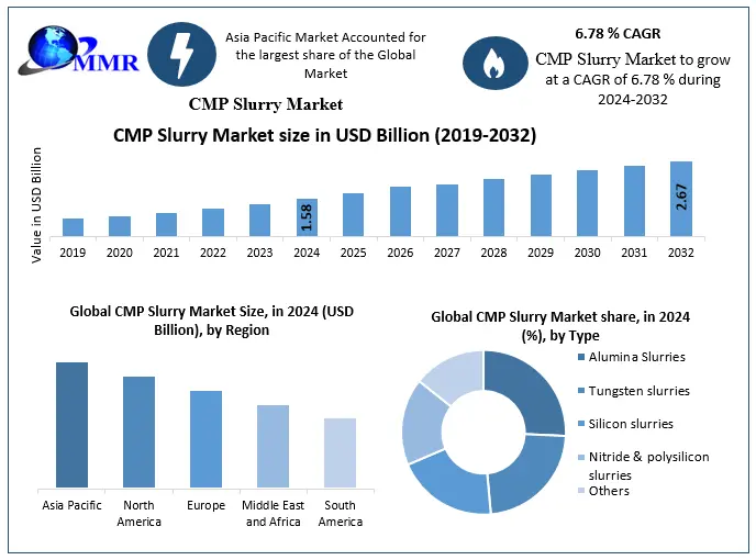
9. CMP Slurry Market Outlook & Industry Trends
The global CMP slurry market was valued at approximately $3.2 billion in 2024 and is projected to grow at a compound annual growth rate (CAGR) of 7.4% through 2032, driven by accelerating adoption of advanced logic nodes, 3D NAND capacity expansion, and rapid growth in advanced packaging. A full analysis of market size, segmentation, and competitive dynamics is covered in our CMP Slurry Market Size, Growth & Forecast 2025–2032 report.
9.1 Key Growth Drivers
- Advanced Logic Scaling (5nm → 2nm): Each new node generation adds 2–5 additional CMP steps per wafer, directly increasing slurry consumption per die. TSMC N2 is estimated to require over 25 CMP operations per wafer.
- 3D NAND Stacking: Each additional NAND layer pair requires at least one additional W CMP step. As manufacturers move from 128-layer to 300+ layer NAND, slurry volume per device grows proportionally.
- Advanced Packaging (CoWoS, SoIC, HBM): Chiplet integration and high-bandwidth memory stacking require precision CMP for TSV reveal, wafer thinning, and redistribution layer (RDL) planarization — a fast-growing new demand segment.
- Geopolitical Diversification: The U.S. CHIPS Act and European Chips Act are driving greenfield fab investments in the U.S., Europe, and Japan, creating new geographic demand centers for semiconductor-grade CMP consumables.
9.2 Competitive Dynamics
The CMP slurry market is characterized by high barriers to entry — driven by stringent qualification requirements at leading fabs, proprietary abrasive synthesis technology, and multi-year application development cycles. However, Chinese domestic suppliers are gaining meaningful market share in mature-node applications (≥28nm), supported by preferential procurement policies at domestic fabs, shorter lead times, and increasingly competitive formulation capabilities.
Among the notable domestic players, Jizhi Electronic Technology Co., Ltd., headquartered in Wuxi, Jiangsu — one of China’s most active semiconductor industrial clusters — has established itself as a focused CMP polishing slurry specialist. Wuxi’s proximity to major domestic wafer fabs and its well-developed semiconductor supply chain ecosystem give Jizhi a logistical and technical support advantage for customers in eastern China. Jizhi represents the broader trend of Chinese slurry manufacturers closing the technology gap with established global leaders. Their collective advancement into higher-node applications is an area to watch closely over 2025–2027 as domestic fab capacity continues to expand under the national semiconductor self-sufficiency push.
10. How to Select the Right CMP Slurry for Your Application
Selecting a CMP slurry is a multi-dimensional engineering decision. The following framework guides process engineers through the key decision variables:
- Define the Target Film: Identify the film to be removed (SiO₂, Cu, W, Si₃N₄, Ta, poly-Si, Co, etc.) and the underlying stop-layer film. This determines the primary abrasive type and chemical package.
- Establish MRR and Selectivity Requirements: What removal rate (Å/min) is needed for your throughput target? What selectivity ratio (target:stop) is required to hit your remaining film thickness window?
- Set Defectivity Budget: Consult your device yield model to determine maximum allowable scratch density, LPD count, and contamination levels. Higher defectivity budgets allow more aggressive slurry chemistries.
- Evaluate Slurry-Pad Compatibility: Shortlist slurries that are known to perform with your installed CMP tool platform and pad type. Mixed-supplier combinations (e.g., new slurry + existing pad) require systematic DOE validation.
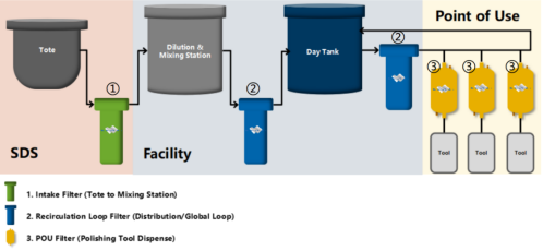
- Assess Handling & Filtration Requirements: Some slurries — particularly ceria and alumina-based products — are prone to settling and require point-of-use filtration (POU, typically 0.5–2 µm) and recirculation. Slurry handling infrastructure costs should be factored into TCO. See our guide on CMP Slurry Filters: Why They Matter & How to Choose.
- Run Qualification Wafers: Qualify under your production process conditions — tool, pad, conditioner, flow rate, pressure, temperature — before full production deployment. Establish statistical process control (SPC) limits for incoming slurry critical parameters.
💡 Pro Tip: Slurry Storage & Handling
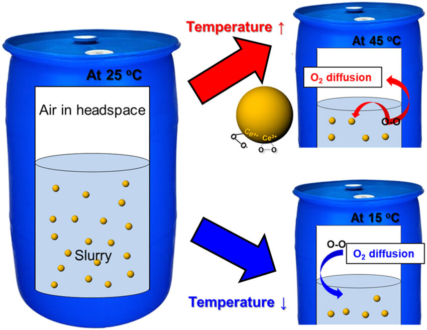
CMP slurry shelf life is strongly temperature-dependent. Most slurries should be stored at 15–25°C in UV-opaque containers; freezing or overheating irreversibly damages colloidal stability. Always follow supplier-specified storage protocols. For a complete handling guide, see our article on CMP Slurry Storage, Handling & Safety.
11. CMP Slurry Quality Control & Defect Management
Consistent CMP performance requires rigorous quality control at every stage — from raw material synthesis through delivery and point-of-use. A robust incoming quality control (IQC) program for CMP slurry typically includes the following measurements on every production lot:
- Particle Size Distribution (PSD) via Dynamic Light Scattering (DLS) or Multi-Angle Light Scattering (MALS): D50, D99, and LPC (large particle count, typically particles >0.5 µm) are the most critical parameters for scratch risk management.
- pH Measurement: pH excursion beyond ±0.2 from specification can destabilize abrasive dispersion or alter chemical removal selectivity. Certified pH meters with traceable calibration standards are required.
- Zeta Potential: A measure of electrostatic repulsion between abrasive particles. Zeta potential below ±25 mV typically indicates risk of agglomeration; most stable slurries target ±40–60 mV.
- Oxide Removal Rate (Reference Wafer Test): Incoming MRR verification on thermal oxide blanket wafers provides a direct functional check of slurry chemical activity.
- Metal Ion Concentration (ICP-MS): Fe, Na, K, Ca, and other trace metal contaminants must meet ppb-level specifications to avoid device gate oxide reliability issues.
Beyond incoming inspection, effective defect management involves correlating post-CMP wafer inspection data (KLA or Hitachi inspection tools) with incoming lot parameters to detect statistical signals before a lot reaches production wafers. A detailed treatment of defect root cause analysis — including scratch morphology classification, particle agglomeration failure modes, and pH-induced instability — is available in our guide to CMP Slurry Defects Analysis & Quality Control.
📚 Explore Our Complete CMP Slurry Resource Library
This guide is the hub of our CMP slurry knowledge base. Dive deeper into any specific topic with the articles below:
12. Frequently Asked Questions About CMP Slurry
What is the difference between CMP slurry and polishing compound?
How long does CMP slurry last (shelf life)?
Can CMP slurry be reused or recycled?
What causes scratches in CMP, and how does slurry formulation affect scratch risk?
What is ceria slurry used for in semiconductor manufacturing?
How is CMP slurry disposed of safely?
Ready to Source High-Performance CMP Slurry?
Talk to our application engineers about qualification support, sample requests, and volume pricing for your specific CMP process requirements.
Get in Touch with Our CMP Team →Conclusion
CMP slurry is far more than a polishing liquid — it is a precision-engineered specialty chemical that enables the nanometer-scale surface planarity on which every advanced semiconductor device depends. As process nodes shrink below 3nm and device architectures evolve into three-dimensional stacks, the formulation science behind CMP slurry becomes ever more sophisticated, and the selection of the right slurry — and the right supplier partner — becomes ever more consequential for fab yield and competitiveness.
Whether you are a process engineer qualifying a new slurry for a sub-5nm application, a materials procurement manager evaluating alternative suppliers, or a technology analyst mapping the CMP consumables landscape, we hope this guide has provided a solid technical foundation. Explore the linked cluster articles for deeper treatment of each subtopic, or contact our technical team directly to discuss your specific process requirements.