Stay informed about the latest developments, important announcements and corporate news of Jizhi Electronics. We are committed to sharing the company’s growth journey and key milestones with our customers.
← Back to: Diamond Dicing Blades: The Complete Guide Selecting the wrong bond type for your dicing application is one of the most common — and costly — mistakes in ...
Whether you’re singulating silicon wafers for advanced ICs, slicing SiC substrates for EV power devices, or cutting ceramic packages for RF modules, the performance of your dicing blade directly determines ...
Contamination Control A single glass fiber fragment from a degraded polishing template carrier plate can scratch dozens of wafers before it is identified. Contamination control starts at template manufacturing — ...
Fab Operations Best Practices Polishing templates are precision consumables — not commodity items to be used and discarded without discipline. The fabs that achieve the longest service life per template ...
Troubleshooting Guide Before adjusting your process recipe, check the template. Five specific template conditions account for the majority of edge profile excursions in production — and each one has a ...
Glass & Ceramic Substrates Glass and ceramic substrates span the widest thickness range, the most varied chemistries, and the most diverse geometries of any substrate category. Getting the polishing template ...
Compound Semiconductor Substrates III-V compound semiconductors and sapphire demand polishing templates that silicon engineers rarely encounter: softer pads to protect fracture-prone crystals, chemically resistant carrier plates for bromine and acid ...
SiC Substrate Engineering Silicon carbide is the hardest common semiconductor substrate and demands the most chemically aggressive CMP slurries. Standard polishing templates fail within weeks. This guide covers what SiC ...
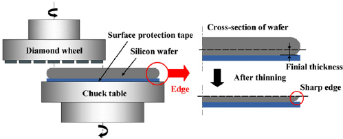
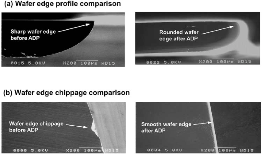
Edge Engineering Guide Every millimeter of edge exclusion zone you eliminate converts directly into additional die area. This guide explains the physics of edge rolloff and the template design parameters ...
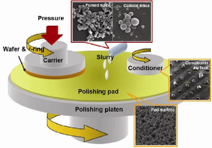
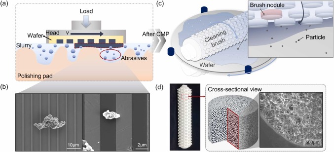
CMP Process Engineering In chemical mechanical planarization, every nanometer of within-wafer non-uniformity has a device yield consequence. This guide explains exactly how polishing template geometry and backing pad design control ...
Material Engineering Guide Two materials. Nearly identical names. Genuinely different performance envelopes. This guide explains exactly when each is the right choice — and when neither is sufficient. By Jizhi ...
Process Technology Comparison Two fundamentally different approaches to holding a wafer during single-side polishing. One has been the industry standard for decades. The other has largely replaced it — and ...