CMP Slurry for SiC Wafer Polishing: Challenges & Solutions
A comprehensive technical guide to CMP slurry selection and process development for silicon carbide substrate polishing — covering the unique challenges of SiC’s extreme hardness, multi-stage polishing strategies, abrasive selection, and surface quality requirements for power device epitaxy.
Silicon carbide (SiC) has emerged as one of the most strategically important semiconductor substrate materials of the 2020s. Its exceptional combination of wide bandgap (3.26 eV for 4H-SiC), high critical electric field (3 MV/cm), high thermal conductivity (4.9 W/cm·K), and high electron saturation velocity makes it the material of choice for power semiconductor devices in electric vehicles, industrial motor drives, renewable energy inverters, and traction applications. SiC device demand has grown at double-digit annual rates since 2020 and shows no signs of decelerating.
But SiC’s extraordinary material properties — the same properties that make it so valuable as a power device substrate — make it one of the most difficult materials to polish to the surface quality required for epitaxial deposition. Understanding why, and knowing how to address these challenges through appropriate CMP slurry selection and process design, is the subject of this article.
1. Why SiC Polishing Is Fundamentally Different
To understand why SiC CMP requires fundamentally different slurry chemistry from silicon, it helps to consider the physical and chemical nature of the polishing challenge. In silicon CMP, the process essentially involves the hydroxide-assisted dissolution of a silica-like surface layer — a relatively soft, chemically reactive system that responds well to alkaline colloidal silica slurries. The silicon surface is chemically active, and the combination of mechanical abrasion and chemical softening makes the process efficient at commercially useful removal rates.
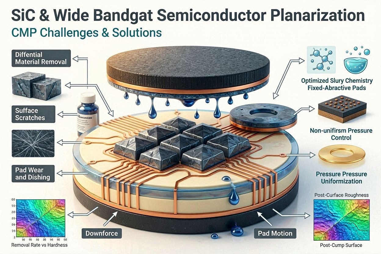
SiC presents an entirely different picture. The Si–C bond that holds the silicon carbide crystal together is extremely strong — bond dissociation energy of approximately 435 kJ/mol, compared to 323 kJ/mol for Si–O in silica. The crystal structure is dense and hard. The material shows no tendency to dissolve or soften under the alkaline conditions that work so well for silicon. And at Mohs 9.5, SiC is harder than any conventional abrasive except diamond — meaning that silica (Mohs 7) and even alumina (Mohs 9) provide only marginal hardness advantage over the target material, resulting in negligible mechanical abrasion at practical process conditions.
2. The SiC Substrate Market: Scale and Growth
The urgency of solving SiC polishing challenges is driven by the scale of the market opportunity. 4-inch and 6-inch SiC wafer production is now well-established, and the industry is actively ramping 8-inch SiC wafer capability. Leading SiC substrate suppliers including Wolfspeed, STMicroelectronics, Rohm, Onsemi, and several Chinese suppliers are investing billions in new SiC substrate and epitaxy capacity.
Each SiC wafer requires multiple polishing steps — from initial wire-saw slicing damage removal through final epi-ready finishing — and each step consumes CMP slurry. The total CMP slurry demand from the SiC market is growing proportionally with wafer production volume, creating a significant and fast-growing market for suppliers with genuine SiC-specific formulation capability. This is one of the segments where JEEZ has invested most heavily in application-specific slurry development.
3. Core CMP Challenges for SiC
When silicon CMP slurries (colloidal silica, pH 10–11) are applied to SiC, removal rates of just 2–5 nm/min are typical — compared to 50–300 nm/min for the same slurry on silicon. At these rates, polishing a single SiC wafer to specification would require many hours per stage, making it completely impractical for production. Even alumina-based slurries, with their greater hardness, deliver only 10–30 nm/min on SiC without chemical assistance — better, but still inadequate for cost-effective manufacturing.
SiC exists in multiple polytypes (4H, 6H, 3C are the most commercially relevant) with different crystal face orientations: the silicon face (Si-face), the carbon face (C-face), and the a-face. These faces have dramatically different chemical reactivity and respond differently to the same slurry formulation. The 4H-SiC Si-face — the most important for power MOSFET devices — is relatively inert to most chemical systems, while the C-face is more reactive. Slurry development must account for the specific polytype and face orientation being polished.
Achieving practical removal rates on SiC requires either very hard abrasives (diamond) or aggressive chemical assistance. Both approaches increase scratch defect risk. Diamond particles, unless very carefully size-controlled and process-optimized, can cause deep scratches in SiC that are extremely difficult to remove in subsequent stages and that eliminate the wafer for epitaxial use. Managing the trade-off between throughput and surface quality is the central process development challenge in SiC CMP.
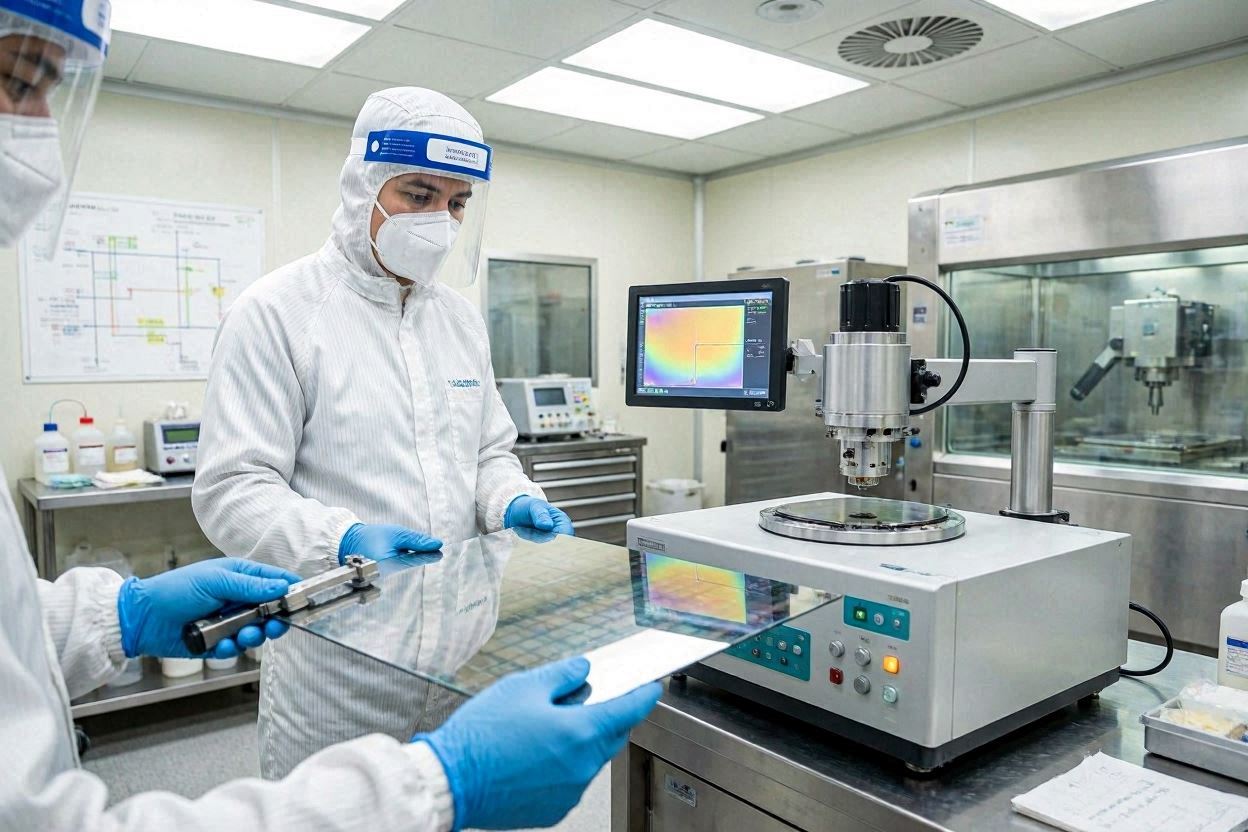
Wire-saw slicing of SiC boules introduces a layer of subsurface crystal damage (micro-cracks, dislocations) that extends 5–20 µm below the sliced surface. This damage layer must be completely removed before epitaxial deposition, because any remaining subsurface damage propagates as crystal defects into the epitaxial layer and degrades device breakdown voltage and leakage current. Confirming complete subsurface damage removal requires selective etching and defect inspection — making this a quality control challenge as well as a process engineering one.
4. Multi-Stage Polishing Strategy
No single slurry formulation can address all stages of SiC wafer preparation efficiently. The industry has converged on a multi-stage approach that uses different slurry types at each stage, optimized for the primary objective of that stage:
Removes wire-saw damage and brings wafer to flatness specification. Highest material removal requirement.
Removes coarse stage damage, improves flatness and roughness to enable final polishing. Transitional stage.
Achieves epi-ready surface quality. Zero scratch tolerance. Surface roughness is the primary metric.
5. Abrasive Selection for Each Stage
Stage 1 and 2: Diamond Abrasives
For coarse and intermediate stock removal on SiC, diamond is the only abrasive that provides the hardness margin needed for practical removal rates. Synthetic monocrystalline diamond particles in the 0.5–15 µm range are used, with smaller particles at finer stages to progressively reduce surface roughness while maintaining useful throughput.
The most critical quality parameter for diamond slurries used on SiC is the maximum particle size — a single oversized diamond particle can cause a scratch that penetrates deep into the SiC crystal and is nearly impossible to remove in subsequent polishing stages without losing excessive material. Diamond slurry suppliers who provide tight D99 (99th percentile) particle size specifications and use high-quality filtration in manufacturing are strongly preferred for SiC applications.
Stage 3: Ceria or Chemically Enhanced Silica
The final CMP stage for SiC requires transitioning away from diamond abrasives entirely — diamond’s hardness, which is necessary for removal rate in earlier stages, becomes a liability when Ra < 0.3 nm is the target and zero scratches are required. Two approaches have been validated for SiC final finishing:
- Ceria-based slurries with oxidizing additives: The combination of Ce⁴⁺’s chemical reactivity with SiC’s oxidized surface layer (SiO₂ + CO₂ decomposition products) and the mechanical action of ceria particles can achieve 10–50 nm/min on 4H-SiC Si-face with acceptable surface quality when optimized oxidizer concentrations are used.
- Colloidal silica with strong oxidizer: Hydrogen peroxide (5–15%), potassium permanganate, or sodium hypochlorite can oxidize the SiC surface to a softer SiO₂-like layer that is then removable by colloidal silica at alkaline pH. The challenge is maintaining adequate oxidation rate on the highly stable SiC surface while avoiding unacceptable surface roughness or contamination from the oxidizer decomposition products.
6. Chemical Assistance: The Key to Practical MRR
The central insight of effective SiC CMP chemistry is that the SiC surface must be chemically converted to a softer, more reactive form before — or simultaneously with — abrasive contact. Without chemical assistance, even diamond particles make negligible progress on the pristine SiC crystal surface at normal polishing pressures.
The two primary chemical conversion mechanisms used in SiC CMP are:
- Thermal oxidation analog via chemical oxidation: Strong oxidizers (H₂O₂, KMnO₄, or NaOCl) convert Si–C surface bonds to Si–O and C–O products. The silicon-containing oxidation product is essentially SiO₂ — soft and removable by abrasive contact. The carbon-containing products (CO₂ gas or dissolved carbonate) are removed naturally. This mechanism effectively converts the hard SiC surface into a softer SiO₂ analog at the polishing interface, enabling much higher effective removal rates.
- Electrochemical-assisted CMP (ECMP): An emerging approach that applies an anodic potential to the SiC wafer surface during polishing, electrochemically accelerating the surface oxidation rate beyond what chemical oxidizers alone can achieve. ECMP is not yet widely deployed in production but has demonstrated MRR improvements of 5–10× over purely chemical approaches on 4H-SiC, at the cost of tool complexity and current distribution uniformity challenges.
Research note: The oxidizer concentration in SiC CMP slurries must be carefully balanced. Too little oxidizer results in insufficient surface conversion and low MRR. Too much oxidizer can cause rapid uncontrolled surface dissolution, excessive surface roughness, or contamination from oxidizer decomposition products. The optimal concentration window is typically determined experimentally for each slurry-tool-pad-SiC polytype combination.
7. Surface Quality Requirements for Epi-Ready SiC
The surface quality specification for an epi-ready SiC wafer is substantially more demanding than for epi-ready silicon. This reflects the fact that crystal defects in SiC epitaxy propagate more readily from substrate surface imperfections, and that the high electric field operation of SiC power devices makes any surface-originated crystal defect a potential reliability risk:
| パラメータ | Epi-Ready 4H-SiC Specification | Epi-Ready Si (Reference) | Measurement Method |
|---|---|---|---|
| 表面粗さ Ra | <0.3 nm (5×5 µm AFM) | <0.1 nm | AFM (5×5 µm scan) |
| スクラッチ密度 | Zero scratches visible (KLA) | Zero scratches | Bright-field laser inspection |
| Subsurface damage | Not detectable by selective etch | Not detectable | KOH etch + optical microscopy |
| Bow / Warp | <25 µm (4-inch wafer) | <10 µm | Capacitance mapping |
| 金属汚染 | <1×10¹⁰ atoms/cm² (total metals) | <1×10¹⁰原子/cm²。 | VPD-ICPMS |
| Particle count (>0.3 µm) | <20 per wafer | <10/ウェハ | Laser surface scanner |
Critical point: Meeting the Ra specification is necessary but not sufficient for an epi-ready SiC surface. Subsurface damage is essentially invisible to surface roughness measurement — a wafer can have Ra < 0.3 nm and still contain a subsurface damage layer that will propagate crystal defects into the epitaxial layer. Confirming subsurface damage removal requires a dedicated etch-and-inspect step that is separate from surface roughness characterization.
8. Key Process Parameters and Typical Values
| パラメータ | Stage 1 (Diamond coarse) | Stage 2 (Diamond fine) | Stage 3 (Ceria/SiO₂ finish) |
|---|---|---|---|
| Abrasive type | Diamond 6–15 µm | Diamond 0.5–3 µm | Ceria 50–200 nm or Colloidal SiO₂ |
| 酸化剤 | H₂O₂ 1–5% | H₂O₂ 2–8% | H₂O₂ 5–15% or KMnO₄ |
| pH range | 3–7 (acidic–neutral) | 4-8 | 8–11 (alkaline) |
| Downforce | 3–8 psi | 2–5 psi | 1–3 psi |
| Typical MRR (4H-SiC Si-face) | 500–2,000 nm/min | 50–200 nm/min | 10–50 nm/min |
| Target exit Ra | <10 nm | <2 nm | <0.3 nm |
Process note: All parameter ranges above represent typical values from open literature and industry practice as of May 2026. Actual optimal values for your specific process will depend on wafer polytype and face orientation, tool type, pad selection, conditioner recipe, and slurry formulation. Process development on your actual equipment is always required. For abrasive science background, see: CMP Slurry Abrasives Explained: Silica vs Alumina vs Ceria.
9. JEEZ SiC CMP Slurry Solutions
JEEZ SiC Polishing Slurry Portfolio
JEEZ has developed dedicated CMP slurry formulations for all three stages of the 4H-SiC wafer polishing sequence. Our SiC slurry development program was initiated in response to customer demand from the rapidly growing domestic Chinese SiC substrate and device manufacturing industry, where qualified local consumable sources for specialized applications were — and in many cases remain — limited.
Our Stage 3 ceria finishing slurry uses a proprietary oxidizer package that has been optimized for the 4H-SiC Si-face — the surface orientation relevant for the majority of power MOSFET and Schottky diode devices. The formulation achieves consistent Ra < 0.3 nm and zero-scratch results on properly prepared (Stage 2 complete) SiC wafers under standard process conditions, and our application engineering team provides full process setup and optimization support during customer qualification.
While we do not have public customer case studies to share, our formulation characterization data (particle size distribution, zeta potential stability, MRR on reference SiC substrates, and LPC measurements) is available under NDA for qualified prospective customers.
For context on how SiC CMP fits within the broader CMP slurry landscape, see our complete supplier guide: Top CMP Slurry Manufacturers: Global Supplier Guide 2026. For the general CMP slurry selection framework, see: How to Choose a CMP Slurry: Selection Guide for Semiconductor Engineers.
Developing a SiC CMP Process?
JEEZ’s SiC polishing slurry team can support your process development from initial formulation selection through qualification and production. Contact us to discuss your polytype, face orientation, throughput requirements, and surface quality targets.
Contact Our Experts →