The Complete Guide to Silicon Wafer Polishing
From the physics of chemical-mechanical planarization to slurry formulation, defect management, and cost control — the definitive reference for process engineers, materials buyers, and fab technologists working with polished silicon substrates in 2026.
- What Is Silicon Wafer Polishing?
- How Chemical Mechanical Polishing Works
- The Polishing Process: Step by Step
- Single-Side vs. Double-Side Polishing
- CMP Slurry: Chemistry and Selection
- Colloidal Silica vs. Alumina Abrasive
- Polishing Pads: Materials and Design
- Quality Metrics: TTV, SFQR, Ra, LPD
- Achieving Sub-Nanometer Surface Roughness
- Common CMP Defects and Prevention
- 300mm Wafer Polishing: Challenges and Uniformity
- Post-CMP Cleaning
- CMP Cost Optimization
- Silicon vs. SiC Wafer Polishing
- Related In-Depth Articles
- よくある質問
What Is Silicon Wafer Polishing?
Silicon wafer polishing is the critical surface preparation process that transforms a rough, freshly sliced silicon disk into a mirror-flat, atomically smooth substrate suitable for advanced integrated circuit fabrication. Without polishing, the residual surface damage from wire-saw slicing and mechanical lapping would make it impossible to deposit reliable gate oxides, grow defect-free epitaxial layers, or achieve the photolithographic overlay accuracy demanded by modern logic and memory nodes.
At its core, silicon wafer polishing combines two simultaneous mechanisms — mechanical abrasion and chemical reaction — to remove material from the wafer surface in a controlled, uniform manner. The process must achieve three goals that are in constant tension: wafer-level flatness measured in fractions of a micrometer, surface smoothness measured in fractions of a nanometer, and freedom from particles and crystalline defects. Achieving all three concurrently at the tolerances required for single-digit nanometer device nodes demands precise control of slurry chemistry, pad properties, applied pressure, rotation speed, temperature, and post-process cleaning.
Chemical mechanical planarization (CMP) is the dominant polishing technology in commercial silicon wafer manufacturing as of June 2026. First applied to silicon substrates in the late 1980s, CMP has evolved into a highly refined multi-stage process capable of delivering wafer front surfaces with a root-mean-square roughness (Rq) below 0.1 nm — smoother than almost any other industrially produced surface.
Polished silicon wafers underpin every major segment of the semiconductor market: leading-edge logic (sub-5 nm FinFET and gate-all-around nodes), advanced DRAM, 3D NAND flash, MEMS inertial sensors, RF front-end modules, SiGe HBTs for millimeter-wave communications, and silicon photonic waveguide chips. As device architectures grow more complex and feature dimensions continue to shrink, polishing specifications tighten further — making deep expertise in silicon wafer CMP one of the most strategically important competencies in the semiconductor supply chain.
How Chemical Mechanical Polishing (CMP) Works
Chemical mechanical polishing achieves wafer planarization by combining two simultaneous material-removal mechanisms: a chemical reaction that weakens or oxidizes the wafer surface layer, and a mechanical action that physically shears away the weakened material through abrasion. Neither mechanism alone can deliver the combination of high removal rate, global flatness, and low defect density that CMP achieves when the two are properly balanced.
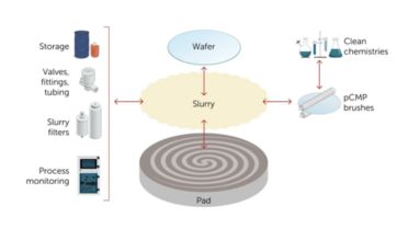
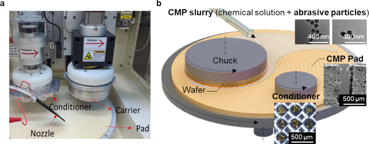
In a standard CMP configuration, the silicon wafer is mounted face-down on a rotating carrier head using a flexible membrane that applies controlled, zone-specific downward pressure. A retaining ring surrounding the wafer prevents it from sliding off the pad during polishing. The wafer presses against a rotating polishing pad mounted on a large circular platen. A polishing slurry — containing nanoscale abrasive particles suspended in an alkaline chemical solution — is continuously delivered to the pad surface through a dispense arm.
The chemical component of the slurry (typically an alkaline solution at pH 10–11 for silicon) promotes the continuous formation of a thin, hydrated silicon oxide layer (SiO₂·nH₂O) at the wafer surface. This chemically modified surface layer is mechanically softer than bulk crystalline silicon and is progressively sheared away by the abrasive particles as the wafer and pad move relative to each other. The rate of material removal follows a modified Preston equation, which relates removal rate to the applied pressure, the relative velocity between wafer and pad, and a process constant that captures slurry reactivity and pad mechanics.
One of the most important properties of CMP is its inherent self-planarizing behavior: protruding topographic features experience higher local contact pressure and therefore a higher removal rate than recessed areas. Over time, this differentially removes high spots and flattens the surface toward the global mean plane — which is precisely the outcome required to correct wafer-level bow, warp, and thickness variation introduced by upstream slicing and lapping operations.
The Silicon Wafer Polishing Process: Step by Step
Silicon wafer polishing is one stage within a carefully sequenced multi-step manufacturing process that begins with a silicon ingot and ends with an inspected, specification-compliant substrate. Understanding how each step prepares the surface for the next — and how upstream process choices propagate into downstream polishing outcomes — is essential for effective process engineering and troubleshooting.
- Single-Crystal Ingot Growth High-purity silicon is melted and a single-crystal ingot is pulled using the Czochralski (CZ) method or, for ultra-low-defect substrates, the float-zone (FZ) method. The ingot is then shaped (ground to a cylindrical diameter), oriented by X-ray diffraction, and given a flat or notch to mark the crystal orientation.
- Wire-Saw Slicing A multi-wire saw equipped with diamond-coated wire (or a slurry-feed wire for older equipment) slices the ingot into individual wafers. The cut surfaces are rough (Ra 1–10 μm), wavy, and carry a sub-surface crystalline damage layer 5–20 μm deep from the mechanical cutting stress. All of this damage must be eliminated before device processing.
- Edge Profiling (Beveling) The sharp, fragile edges of the sliced wafer are precision-ground into a standardized chamfer profile (T-shape or R-shape per SEMI standard M1) using a diamond profiling wheel. Edge profiling prevents micro-cracking at wafer edges during handling, reduces particle generation, and ensures uniform pad contact during subsequent polishing.
- Lapping Both wafer surfaces are simultaneously abraded against a flat lapping plate using a free-abrasive slurry of aluminum oxide or silicon carbide in a carrier fluid. Lapping removes 30–60 μm per side, establishes initial global flatness (TTV typically reduced to below 5 μm), and reduces average surface roughness to Ra ~0.3–1 μm. The surface remains matte and mechanically damaged at this stage.
- Chemical Etching The lapped wafer is immersed in a wet etchant to dissolve the sub-surface crystal damage left by lapping. Acidic etch (HF/HNO₃/CH₃COOH, isotropic) removes 10–30 μm per side uniformly; alkaline etch (KOH, anisotropic) removes damage selectively along crystal planes and leaves a slightly textured surface. The choice between acid and alkaline etching affects downstream surface roughness and defect density.
- Double-Side Polishing (DSP) — Rough CMP The wafer is loaded into thin, precisely machined carrier plates within a double-side CMP machine, which simultaneously polishes both the front and back surfaces. Using a hard polyurethane pad and a relatively aggressive colloidal silica slurry, the DSP step removes 10–20 μm per side, establishes the tight global flatness parameters (TTV, bow, warp) demanded by lithography tools, and produces both surfaces with a Ra below ~0.5 nm. This is the step that defines the wafer’s geometric quality class.
- Single-Side Final Polish (Finish CMP) The front (device) surface is given a final, ultra-low-removal-rate CMP step — typically removing less than 1.5 μm total — using a soft polyurethane pad and a dilute, fine-particle (or abrasive-free) alkaline slurry. Chemical action dominates mechanical abrasion in this stage. The objectives are to eliminate haze, reduce LPD count to specification, and achieve the sub-0.1 nm Rq required for epitaxial growth or high-k dielectric deposition. The back surface is protected by the vacuum or wax carrier during this step.
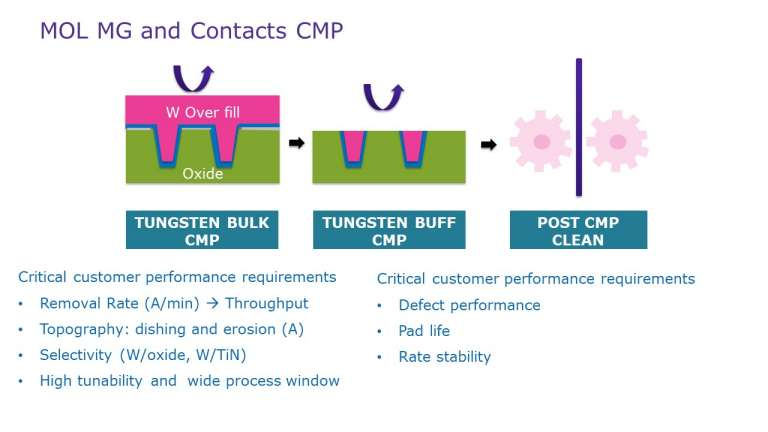
- Post-CMP Cleaning The polished wafer carries residual slurry particles, organic additives, dissolved silicon species, and trace metallic contaminants. A multi-chemical cleaning sequence removes all residues to the sub-ppb level required for device processing. This step is covered in detail in the Post-CMP Cleaning section of this guide.
- Metrology and Final Inspection The cleaned wafer is measured for total thickness variation (TTV), site flatness (SFQR), surface roughness (Ra, Rq, haze), and defect density (LPD count using a laser-scanning surface inspector such as the KLA Surfscan SP series). Wafers meeting all specification limits are packaged in front-opening unified pods (FOUPs) or traveler boxes under controlled-atmosphere conditions for shipment.
Single-Side Polishing vs. Double-Side Polishing
One of the most consequential process architecture decisions in silicon wafer polishing is whether to use single-side polishing (SSP), double-side polishing (DSP), or a combination of both. The two approaches differ in geometry, surface outcomes, equipment requirements, and application suitability.
Double-Side Polishing (DSP)
- Polishes front and back surfaces simultaneously via carrier plates
- Produces superior global flatness (TTV <0.5 μm on 300mm)
- Excellent bow and warp control through geometrically constrained polishing
- Both surfaces processed in a single pass — high throughput
- Industry standard for 200mm and 300mm prime-grade production wafers
- Requires precisely machined carrier plates matched to wafer thickness
片面研磨(SSP)
- Polishes the front (device) surface only
- Wafer held on carrier block by vacuum or thermoplastic wax
- Better local planarity (SFQR) and lower LPD count than DSP alone
- Lower equipment cost; suitable for R&D and small-batch production
- Used as the final finish step after DSP in production flows
- Standard for test, monitor, and many specialty silicon wafer grades
In leading-edge 300mm production fabs, the standard approach combines both methods: a DSP step for global flatness control, followed by an SSP finish polish that eliminates any haze and residual micro-roughness on the device surface. This hybrid sequence exploits the complementary strengths of each method — DSP establishes the geometric foundation, and SSP delivers the surface quality. Understanding the trade-offs between these approaches is essential when specifying wafer polishing equipment, slurry, or pad procurement.
Full comparison: Single-Side vs. Double-Side Polishing — Which Is Right for Your Wafer?CMP Slurry: Chemistry, Composition, and Selection
Of all the consumables in the silicon wafer polishing process, the CMP slurry has the most direct and immediate influence on removal rate, surface roughness, LPD count, and overall wafer quality. Selecting the wrong slurry — or using the right slurry under suboptimal conditions — can simultaneously degrade every major quality metric. Getting slurry selection right is therefore a process engineering decision, not merely a procurement one.
What CMP Slurry Is Made Of
A polishing slurry engineered for silicon wafer CMP is an aqueous colloidal dispersion designed to deliver four simultaneous functions during polishing:
- Chemical reactant: An alkaline base — typically potassium hydroxide (KOH), tetramethylammonium hydroxide (TMAH), or ammonium hydroxide — maintains pH in the range of 9.5–11.5, promoting the continuous formation of a hydrated silicon oxide (SiO₂·nH₂O) surface layer that is chemically softer and more easily removed than bulk Si.
- Abrasive phase: Nanoscale particles — most commonly colloidal silica (20–150 nm) or fumed silica — provide the mechanical component of material removal by physically abrading the softened surface layer as they pass between the pad asperities and the wafer.
- Colloidal stabilizer: Dispersants, pH buffers, and sometimes steric polymer layers keep abrasive particles separated in suspension. Particle agglomeration produces clusters larger than 500 nm that act as “killer particles” — the primary source of scratch defects.
- Surface passivation agents: Some formulations include non-ionic surfactants or chelating agents (EDTA, citric acid) that adsorb onto the freshly polished silicon surface, preventing re-deposition of dissolved silicon species and metallic contaminants from the polishing environment.
Rough Polish vs. Final Polish Slurry: Key Differences
Silicon wafer polishing typically uses at least two distinct slurry formulations tuned for different stages of the process:
| パラメータ | Rough Polish Slurry (DSP) | Final Polish Slurry (SSP) |
|---|---|---|
| Primary objective | Stock removal and global flatness | Haze elimination and sub-nm surface quality |
| Abrasive type | Colloidal silica (larger) or alumina | Colloidal silica (small, monodisperse) or abrasive-free |
| Typical particle size | 80–150 nm | 20–50 nm |
| Abrasive concentration | 5–15 wt% | 0.1–2 wt% (or zero) |
| pH range | 10.5–11.5 | 9.5–11.0 |
| Typical removal rate | 300-800 nm/分 | 20–100 nm/min |
| Pad type | Hard polyurethane (IC1000-type) | Soft, porous polyurethane (Suba-type) |
| LPD priority | Secondary | Critical (<30 @ 35 nm detection on 300mm) |
At Jizhi Electronic Technology Co., Ltd. (JEEZ), our engineers formulate CMP polishing slurries specifically optimized for both polishing stages in silicon wafer manufacturing. Our final-polish colloidal silica products are designed to achieve LPD counts below 30 at the 35 nm detection threshold on 300mm prime-grade wafers, with haze levels below 0.03 ppm. 技術チームへのお問い合わせ to discuss your process requirements or request a sample evaluation.
Full guide: CMP Slurry for Silicon Wafer — Types, Selection & Best PracticesColloidal Silica vs. Alumina: Choosing the Right Abrasive
The abrasive component of a CMP slurry is one of the most consequential formulation choices in the entire polishing process. For silicon wafer applications, the two principal abrasive families are colloidal silica (SiO₂) and alumina (Al₂O₃), each offering a different balance between removal rate, surface quality, and defect risk.
コロイダルシリカ is by far the most widely used abrasive for silicon wafer CMP, particularly in the finish polish stage. Its particles are spherical, narrowly size-distributed, and chemically compatible with silicon — both workpiece and abrasive share the same elemental composition (silicon and oxygen), enabling a true chemical-mechanical synergy. The chemical similarity means that colloidal silica particles can actively participate in the surface condensation reactions forming the removable SiO₂·nH₂O layer, making the combined action more efficient than mechanical abrasion alone. The silica’s relatively low hardness (Mohs ~7) also minimizes the risk of deep scratch defects and sub-surface crystal damage. The result is an ultra-smooth, low-haze surface with excellent LPD performance — which is why colloidal silica dominates all final-polish silicon applications in 2026.
アルミナ (Al₂O₃) offers significantly higher material removal rates — valuable in rough polishing, aggressive stock-removal, or substrate lapping stages where throughput matters more than surface quality. However, alumina particles are harder (Mohs 9) and more angular than colloidal silica, which substantially increases the risk of micro-scratches, surface haze, and sub-surface crystal damage. For this reason, alumina-based slurries are almost never used for final silicon surface polishing in advanced device fabs, though they remain useful for rough-grinding and specific hard-substrate applications such as sapphire and SiC.
Polishing Pads: Materials, Hardness, and Groove Design
The polishing pad is the other half of the consumable pair in CMP. Pad properties — hardness, surface texture, groove geometry, porosity, and wear characteristics — directly control how slurry is transported to the wafer surface, how uniformly contact pressure is distributed, and ultimately how flat and smooth the polished surface becomes. Pad selection is inseparable from slurry selection: the two must be matched to the specific polishing stage and surface quality target.
CMP pads are most commonly manufactured from polyurethane foam or polyurethane-impregnated felt composite, and fall into two broad hardness categories:
Hard pads (Shore D ~60–70, e.g., IC1000-type) are used for rough CMP and DSP stock-removal stages. Their stiffness ensures that surface protrusions experience higher contact pressure than recesses, driving the planarizing mechanism that defines global flatness. Hard pads maintain a relatively stable, consistent removal rate over their lifetime and distribute slurry more uniformly across the wafer diameter, making them ideal for TTV and SFQR control.
Soft pads (Shore A ~50–75, e.g., Suba-type) conform more closely to local surface topography. This conformality reduces the planarizing effect but dramatically decreases the mechanical stress imposed on the wafer surface — making soft pads ideal for the finish polish stage where haze reduction and LPD minimization are the goals rather than geometric correction. Many production processes use a stacked pad configuration: a hard sub-pad for global planarization support with a soft top pad for surface finish quality.
Groove patterns serve a critical fluid-distribution function. Concentric rings, radial channels, X-Y grids, and spiral patterns each create different slurry transport dynamics and affect the uniformity of the liquid film beneath the wafer. Without groove channels, slurry would hydroplane under the wafer, preventing meaningful contact with pad asperities and collapsing the removal rate.
Pad conditioning — the use of a diamond-embedded dresser to periodically scratch and re-texture the pad surface — is essential for maintaining consistent removal rate and uniformity throughout the pad’s service life. Conditioning prevents “pad glazing” (formation of a smooth, non-porous crust from compressed silicon debris and spent abrasive) and must be tuned carefully: over-conditioning shortens pad life, while under-conditioning causes progressive removal rate decay and uniformity drift.
Detailed guide: Polishing Pad Selection for Silicon CMP — Material, Hardness & Groove DesignKey Quality Metrics: TTV, SFQR, Ra, and LPD
Evaluating a polished silicon wafer requires a comprehensive battery of metrology measurements, each capturing a different dimension of surface and geometric quality. Process engineers must understand what each metric quantifies, what its physical origin is, and which process variables control it — because improving one metric in isolation often comes at the expense of another.
| メートル | Full Name | What It Measures | Typical Spec (300mm Prime) |
|---|---|---|---|
| TTV | Total Thickness Variation | Peak-to-valley thickness range across the entire wafer | <1.0 μm |
| お辞儀 | Wafer Bow | Maximum deviation of the median surface from a reference plane (free-standing) | <40 μm |
| ワープ | Wafer Warp | Total deviation range of the median surface (free-standing, both sides) | <60 μm |
| SFQR | Site Flatness Front-surface least-sQuares Range | Peak-to-valley local flatness within each individual lithography site (26×32 mm) | <0.13 μm |
| Ra | Arithmetic Mean Surface Roughness | Average absolute height deviation from the mean surface plane | <0.08 nm |
| Rq (σ) | Root-Mean-Square Roughness | Statistical spread of surface height distribution — more sensitive to rare high peaks | <0.10 nm |
| LPD | Light Point Defects | Count of particles, pits, and anomalies above a detection threshold (laser-scan inspection) | <30 @ 35 nm (300mm) |
| Haze | Surface Haze | Diffuse scattered light intensity from micro-roughness at spatial wavelengths 1–10 μm | <0.03 ppm |
Each metric is sensitive to a different subset of process variables. TTV and SFQR are primarily controlled by the DSP step and depend on pad stiffness, carrier pressure uniformity, and carrier plate flatness. Ra, Rq, and haze are dominated by the finish SSP step and respond strongly to final-polish slurry particle size, abrasive concentration, and pad softness. LPD count is influenced by slurry cleanliness (particularly the presence of oversized particles), pad conditioning quality, and the effectiveness of post-CMP cleaning.
Achieving Sub-Nanometer Surface Roughness
Reaching a root-mean-square roughness (Rq) below 0.1 nm on a silicon wafer front surface is one of the most demanding challenges in industrial surface engineering. At this scale, the “roughness” corresponds to the vertical displacement of less than one silicon lattice plane — the unit cell spacing in the [001] direction is 0.543 nm, meaning an Rq of 0.1 nm represents roughness substantially smaller than a single atomic step. Achieving this level of smoothness consistently across an entire 300mm wafer, wafer after wafer, requires simultaneous optimization of multiple interconnected process parameters.
The following conditions must be met concurrently for reliable sub-nanometer surface roughness:
- Dilute or abrasive-free final polish slurry: Reducing the colloidal silica concentration to 0.1–1.0 wt% — or eliminating abrasive entirely and relying on purely chemical action — minimizes the mechanical contribution that elevates micro-roughness. Abrasive-free alkaline polishing solutions can deliver the smoothest surfaces but require longer process times and well-controlled pH stability.
- Soft finish polishing pad: A pad with Shore A hardness below 60 distributes contact load gently and evenly, preventing the localized high-pressure events between pad asperities and the wafer that generate micro-roughness and scratches.
- Carefully tuned alkalinity: The pH must be high enough to promote silicic acid layer formation but not so high as to drive isotropic chemical etching that roughens the (100) silicon crystal face unevenly along different crystallographic directions.
- Low applied pressure: Reducing the carrier head downforce to below 1 psi (6.9 kPa) for the finish polish stage slows removal rate substantially but enables the chemical component to smooth micro-asperities without introducing new mechanical damage.
- Adequate polish time at low removal rate: An extended finish polish allows the progressive chemical smoothing mechanism to operate fully. This cannot be rushed without sacrificing the final roughness result.
JEEZ final-polish slurry formulations are optimized specifically for this low-pressure, chemistry-dominant polishing regime, delivering reproducible Ra values below 0.07 nm on standard (100) silicon wafers under production conditions.
Process engineering guide: How to Achieve Sub-nm Surface Roughness in Silicon Wafer CMPCommon CMP Defects in Silicon Wafer Polishing
Surface defects introduced during silicon wafer CMP are a leading cause of wafer rejection and yield loss in manufacturing. A single scratch visible on a laser-scanning surface inspector can condemn an entire wafer — representing the complete write-off of all upstream processing costs. Understanding the taxonomy of CMP defects, their root causes, and the process strategies for preventing them is therefore critical knowledge for any wafer polishing engineer.
Defect Types and Their Origins
- Scratch defects: Linear or arc-shaped grooves on the wafer surface, caused by large particles trapped between the pad and the wafer. Sources include abrasive agglomerates formed from colloidal instability, shed pad debris, atmospheric contamination entering the slurry loop, or slurry dispensed after a long idle period when particles have settled. Scratches are the most critical defect type because they cannot be removed without a further polishing step that risks degrading other quality metrics.
- Crystal-originated pits (COPs): Octahedral vacancy-cluster voids present in the bulk Czochralski silicon crystal. During alkaline CMP, the void clusters intersect the surface and the etch-rate difference between the void interior and the surrounding perfect crystal causes them to open into characteristic octahedral pits. COPs are an intrinsic crystal-quality issue but their manifestation can be accelerated by overly aggressive slurry chemistry.
- Surface haze: A diffuse cloudiness across the wafer surface arising from microscale roughness at spatial wavelengths of 1–10 μm, or from thin chemical contamination films left by poorly rinsed slurry additives. Haze elevates the background scattered-light signal on surface inspection tools, masking real defects underneath the noise floor.
- Residual particles (LPD contributors): Slurry abrasive particles that adhere to the polished surface after polishing and are not completely removed by post-CMP cleaning. They appear as positive LPD signals and inflate the defect count.
- Edge roll-off: A systematic reduction in wafer thickness near the outer edge (typically the last 2–5 mm), caused by the polishing pad extending beyond the wafer edge and removing more material in that zone. Edge roll-off increases the edge exclusion zone and reduces the effective die yield at the wafer periphery.
Defect Prevention Strategies
Effective CMP defect control combines slurry quality, process discipline, and cleaning effectiveness:
- Use point-of-use filtration on the slurry supply line to remove particles above 300 nm immediately before the dispense point. JEEZ applies in-process particle size monitoring to all slurry product lots.
- Perform inter-stage quench rinsing with dilute acid or DI water between the rough and finish polishing steps to deactivate and flush residual alkaline slurry before it continues chemically etching the surface.
- Maintain rigorous pad conditioning protocols to prevent pad glazing and the accumulation of debris in the pad surface texture.
- Optimize slurry flow rate: both under-supply (dry spots, particle concentration spikes) and over-supply (turbulence, slurry splashback) degrade defect performance.
- Execute a robust post-CMP cleaning sequence before any surface inspection step.
300mm Silicon Wafer Polishing: Challenges and Uniformity Control
The industry-wide transition from 200mm to 300mm wafers in the early 2000s substantially increased the engineering complexity of silicon wafer CMP. A 300mm wafer has 2.25 times the surface area of a 200mm wafer, and the flatness and defect specifications tightened simultaneously with the diameter increase as device nodes continued to shrink. In June 2026, 300mm remains the volume production standard for leading-edge logic and memory, and many of the most demanding polishing challenges in the industry are concentrated at this wafer size.
Within-Wafer Non-Uniformity (WIWNU)
Within-wafer non-uniformity — variation in removal rate or final polished thickness across the surface of a single wafer — is the most persistent challenge unique to large-diameter CMP. Any slight tilt in the carrier head membrane, non-uniformity in the retaining ring pressure, radial variation in the pad surface condition, or temperature gradient across the platen is amplified as the diameter grows. The result is a radial or azimuthal pattern in removal rate that produces systematic thickness and flatness non-uniformity if not actively compensated.
Modern 300mm CMP tools address WIWNU through multi-zone membrane pressure control: the carrier head is divided into 5–7 independently pressurized concentric zones, each applying a different force to the corresponding annular region of the wafer. Closed-loop in-situ monitoring of removal rate (typically through optical or eddy-current endpoint sensors embedded in the platen) enables real-time zone pressure adjustments to compensate for pad wear and other drift sources.
Retaining Ring and Edge Effects
The retaining ring that encircles the wafer applies a separate, independently controllable downward force on the polishing pad just outside the wafer edge. This “ring load” creates a complex stress pattern in the pad near the wafer periphery that can produce either an edge-fast or edge-slow removal rate signature within the outermost 3–5 mm of the wafer. Controlling retaining ring pressure, ring geometry, ring material (typically ceramic or filled PEEK for minimized metallic contamination), and ring wear state are therefore critical to edge SFQR and to minimizing the edge exclusion zone.
Post-CMP Cleaning: Removing Residues and Protecting the Surface
Even after a technically successful polishing run, a silicon wafer is far from ready for device processing. The polished surface carries a complex mixture of residual slurry abrasive particles, partially reacted silicon dissolution products, organic additives from the slurry formulation, and trace metallic contaminants (principally alkali metals from the slurry base, and transition metals from polishing hardware). Post-CMP cleaning must remove all of these contaminants to the sub-ppb or even sub-ppt level without re-introducing defects, roughening the freshly polished surface, or depositing new ionic contamination.
The most widely used post-CMP cleaning protocol for silicon wafers is a two-chemical RCA-derived sequence, often combined with megasonic acoustic energy for enhanced particle removal:
- SC-1 Clean (APM — Ammonium Peroxide Mixture) A solution of ammonium hydroxide (NH₄OH), hydrogen peroxide (H₂O₂), and ultra-pure deionized water (typical ratio 1:2:10) at 60–80°C. SC-1 removes organic residues by oxidative decomposition, lifts adhered slurry particles by mild surface micro-etching (~0.5 nm Si removal) that undercuts the particles, and exploits electrostatic repulsion — both colloidal silica abrasive and the silicon surface carry a negative zeta potential at SC-1 pH, which aids particle desorption. Megasonic transducers operating at ~1 MHz are frequently applied during SC-1 to provide mechanical energy for dislodging tenacious particles without scratching the surface.
- Deionized Water Rinse A thorough cascade rinse in ultra-pure DI water (resistivity >18.2 MΩ·cm, TOC <1 ppb) between chemical steps prevents chemical carry-over that could compromise the subsequent step’s effectiveness or introduce cross-contamination.
- SC-2 Clean (HPM — Hydrochloric Peroxide Mixture) A solution of hydrochloric acid (HCl), hydrogen peroxide (H₂O₂), and DI water (ratio approximately 1:1:5) at 70–80°C. SC-2 removes metallic ion contamination — particularly alkali metals (Na⁺, K⁺) and transition metals (Fe, Cu, Ni) — by complexation and dissolution into the acidic solution. This step is critical for ensuring the chemical purity of the silicon surface before high-temperature processes such as thermal oxidation.
- Final DI Water Rinse and Spin-Dry A final ultra-pure DI water rinse removes all traces of the SC-2 chemistry, followed by a high-speed centrifugal spin-dry. The drying step must be executed carefully to avoid watermark formation — isolated droplet residues that concentrate dissolved species as they evaporate and leave mineral deposits that appear as LPDs on post-clean inspection.
CMP Cost Optimization: Reducing Slurry Use and Improving Yield
In a high-volume silicon wafer manufacturing environment, CMP consumable costs — primarily polishing slurry and polishing pads — represent a substantial and highly visible fraction of total variable cost per wafer. Slurry alone typically accounts for 30–50% of CMP consumable spending, making slurry process optimization one of the highest-leverage cost-reduction levers available to the wafer manufacturer.
Slurry Consumption Reduction
The most straightforward path to slurry cost reduction is slurry recirculation. Spent slurry collected from the polishing tool drain is passed through a multi-stage filter system to remove large particles (>300 nm), silicon swarf, pad debris, and spent organic additives, and then replenished with a controlled addition of fresh concentrated slurry to restore abrasive concentration and pH. Properly implemented recirculation systems can reduce net fresh slurry consumption by 30–60% with no measurable degradation in surface quality. Not all slurry formulations tolerate recirculation equally well — colloidal stability under repeated filtration cycles and pH re-adjustment varies significantly between products, and JEEZ provides recirculation compatibility data for all product grades.
Slurry flow rate optimization is another accessible lever. Most CMP tools are operated with significant slurry excess — not all of the slurry dispensed onto the platen surface reaches the active wafer–pad contact zone. Systematic optimization of flow rate, dispense point, and pad groove geometry can reduce slurry consumption by 15–25% without process compromise.
Pad Life Extension
Polishing pad lifetime is determined by total material removed and total conditioning cycles. Optimizing the conditioning recipe — the diamond dresser down-force, sweep rate, and conditioning frequency — to balance pad surface refresh against pad wear can extend the number of wafers per pad by 20–40%. Real-time process monitoring (in-situ removal rate sensors, within-wafer uniformity tracking) enables condition-on-demand strategies rather than fixed wafer-count conditioning schedules, further extending pad life without uniformity degradation.
Yield as the Most Powerful Cost Driver
The single most impactful cost lever in wafer polishing is wafer yield. A defect-driven rejection at the polishing inspection step writes off all upstream manufacturing cost — ingot growth, slicing, lapping, etching, and partially completed polishing. Investing in a higher-quality slurry with tighter particle size distribution and superior colloidal stability — even at a modestly higher per-liter cost — typically delivers a strongly positive total-cost-of-ownership outcome through improved yield. JEEZ technical engineers work with customers to model the full cost impact of slurry grade selection on a yield-adjusted per-wafer cost basis.
Cost engineering guide: CMP Cost Optimization — Reduce Slurry Consumption and Improve YieldSilicon Wafer Polishing vs. SiC Wafer Polishing
As the power semiconductor market continues its rapid expansion through 2026 — driven by electric vehicle traction inverters, industrial variable-speed drives, and renewable energy conversion systems — silicon carbide (SiC) wafers have become strategically important substrates alongside traditional silicon. Engineers who are fluent in silicon CMP and are transitioning to SiC substrate processing encounter a fundamentally different set of material challenges.
Silicon is a relatively soft material (Mohs hardness ~7) with moderate chemical reactivity. The alkaline dissolution mechanism in silicon CMP contributes substantially to removal rate, enabling fast, controllable polishing with colloidal silica at modest pressures. SiC, by contrast, is one of the hardest commercially processed materials (Mohs 9–9.5), with extremely strong and chemically resistant Si–C covalent bonds. CMP removal rates on SiC are typically one to two orders of magnitude lower than on silicon under comparable conditions, and achieving a damage-free, epi-ready SiC surface generally requires oxidizing slurry chemistries (incorporating H₂O₂, KMnO₄, or Fenton reagents) combined with harder abrasives (diamond or alumina) at higher pressures and with much longer process times.
The polishing pad selection, process parameter windows, quality metrics (surface step density, basal plane dislocations, micropipe density), and post-polish cleaning protocols all differ significantly between silicon and SiC applications. Understanding these differences at a mechanistic level is essential for any materials or process engineer working across both substrate platforms.
Detailed comparison: Silicon Wafer Polishing vs. SiC Wafer Polishing — Key Differencesよくある質問
The questions below address the most common inquiries from process engineers, fab technologists, and materials procurement professionals regarding silicon wafer polishing.
Need High-Performance CMP Slurries for Silicon Wafer Polishing?
Jizhi Electronic Technology Co., Ltd. (JEEZ) develops and manufactures CMP polishing slurries engineered for silicon wafer applications at every polishing stage — from aggressive DSP stock-removal to ultra-fine finish polish delivering Ra below 0.07 nm. Our technical team offers in-depth process consultation, slurry sample evaluation programs, and total cost-of-ownership analysis tailored to your specific wafer specification and equipment configuration.
Contact JEEZ Technical Team