300mm Silicon Wafer Polishing: Challenges and Uniformity Control
A deep technical guide to the unique challenges of polishing 300mm silicon wafers — within-wafer non-uniformity (WIWNU) sources, multi-zone pressure control, retaining ring optimization, pad management, and endpoint detection strategies for leading-edge production.
Why 300mm CMP Is Fundamentally Different from 200mm
When the semiconductor industry transitioned from 200mm to 300mm silicon wafers in the early 2000s, every CMP challenge scaled — and some scaled non-linearly. A 300mm wafer has 2.25 times the surface area of a 200mm wafer. The polishing head must maintain pressure uniformity across a 300mm disk while correcting for pad wear patterns, retaining ring dynamics, and slurry film non-uniformities that all influence the final thickness and flatness profile. Meanwhile, device node scaling simultaneously tightened flatness and surface quality specifications, creating a confluence of larger diameter and tighter tolerances that defines the 300mm CMP challenge as of June 2026.
This guide from Jizhi Electronic Technology Co., Ltd. (JEEZ) addresses the specific engineering challenges of 300mm silicon wafer polishing — within-wafer non-uniformity control, multi-zone pressure technology, retaining ring optimization, pad management, and edge exclusion minimization. For the complete process context, see our Complete Guide to Silicon Wafer Polishing.
Within-Wafer Non-Uniformity: Definition, Sources, and Measurement
Within-wafer non-uniformity (WIWNU) is the normalized variation in material removal rate or final polished thickness across the surface of a single wafer, expressed as a percentage:
WIWNU (%) = (RR_max − RR_min) / RR_mean × 100
For 300mm prime-grade silicon wafer polishing in the DSP step, typical production targets are WIWNU <2% measured across the wafer minus a 3mm edge exclusion zone. In the SSP finish-polish step, WIWNU must be sufficiently low that the shallow total removal (0.5–1.5 μm) does not translate into measurable TTV or SFQR degradation.
Physical Sources of WIWNU at 300mm
- Pad thickness non-uniformity and wear patterns: As a pad wears during polishing, it develops radial wear patterns driven by the kinematics of the carrier head sweeping across the platen. Worn zones in the pad have different compressibility than fresh zones, creating radial removal rate signatures — typically an edge-fast or center-fast profile — that worsen progressively through the pad’s lifetime.
- Slurry film non-uniformity: The slurry film between pad and wafer is not perfectly uniform in thickness or concentration. Radial variations in slurry transport — governed by pad groove geometry, slurry dispense location, and centrifugal force — create corresponding removal rate variations across the wafer diameter.
- Pressure non-uniformity: Any tilt or non-planarity in the carrier head membrane, retaining ring wear, or polishing head bearing misalignment translates directly into wafer-scale pressure non-uniformity. At 300mm, a 1% variation in average applied pressure corresponds to a ~1% variation in removal rate across the wafer.
- Temperature gradients: CMP is exothermic. The frictional heat generated during polishing creates temperature gradients across the wafer and pad surface, which in turn drive gradients in the chemical reaction rate (slurry temperature affects the silicon oxide formation rate). Temperature uniformity is harder to maintain across larger platen diameters.
Multi-Zone Carrier Head Pressure Control
The most powerful engineering tool for WIWNU correction at 300mm is the multi-zone carrier head. In a multi-zone head, the membrane that contacts the wafer back surface is divided into independently pressurized concentric annular zones — typically 5 to 7 zones on leading-edge 300mm tools from Applied Materials, Ebara, and other equipment suppliers.
Each zone can apply a different downforce to the corresponding annular region of the wafer. By independently adjusting each zone’s pressure, the process engineer can apply more force to under-polishing regions (to increase local removal rate) and less force to over-polishing regions. This active zone-by-zone compensation transforms what would be a fixed, symmetric problem into a dynamically tunable one.
Zone Pressure Optimization Methodology
- Baseline measurement Run a fixed-pressure recipe and measure the post-polish thickness profile across the wafer diameter in fine radial increments (every 5–10 mm). Identify the radial zones where removal rate is too high (thinner) or too low (thicker) relative to target.
- Sensitivity matrix Characterize the response of each wafer radial zone to a unit change in each carrier head pressure zone (1 psi increment). This sensitivity matrix is determined by running a designed experiment (DOE) with systematic zone pressure offsets and measuring the resulting removal profile changes.
- Pressure recipe optimization Use the sensitivity matrix to calculate the zone pressure combination that minimizes WIWNU across all radial zones simultaneously. This is a constrained optimization problem (pressures must remain within tool limits; removal rate must remain within acceptable range).
- Closed-loop control Advanced tools implement closed-loop WIWNU control: in-situ thickness sensors (optical interferometry or eddy current) measure the evolving removal profile during polishing and feed back real-time zone pressure adjustments to maintain target WIWNU throughout the run.
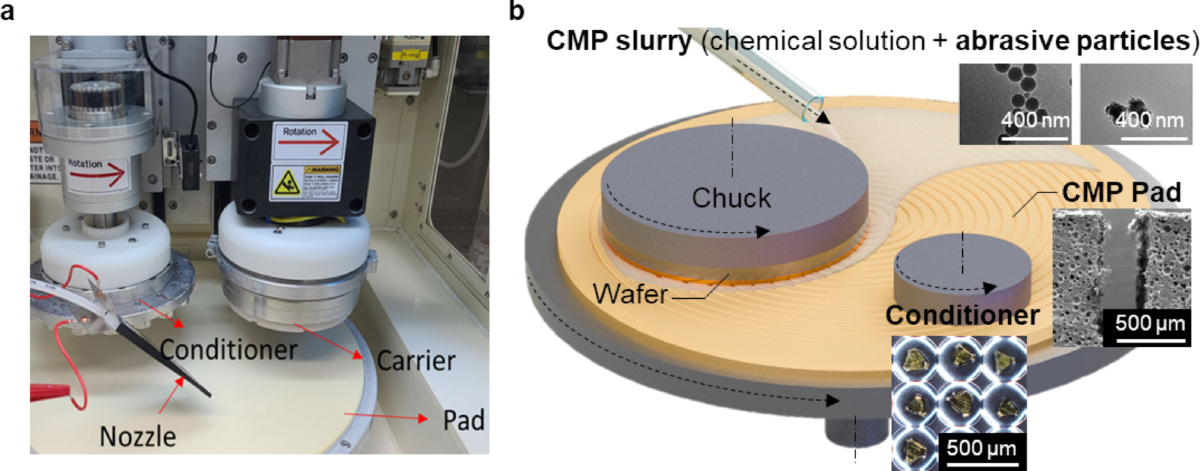
Retaining Ring Design and Optimization
The retaining ring encircles the wafer in the carrier head and performs two functions: it physically prevents the wafer from sliding out from under the head during polishing, and it applies a controllable downforce to the polishing pad surface just outside the wafer edge. This ring load creates a pad deformation pattern that profoundly influences the removal rate in the wafer’s edge zone (outermost 3–5 mm).
Ring Load Effect on Edge Profile
When the retaining ring applies a high load to the pad outside the wafer edge, it “bows” the pad upward at the wafer edge, increasing contact pressure at the wafer periphery → edge-fast removal → edge roll-down (thinner edge). When ring load is insufficient, the pad springs back outside the wafer edge, reducing contact at the periphery → edge-slow removal → edge roll-up (thicker edge). The optimal ring load that minimizes the edge SFQR signature is typically 15–25% higher than the wafer polishing pressure, but varies by pad type, slurry, and wafer diameter.
Retaining Ring Materials
| 素材 | Advantages | Disadvantages |
|---|---|---|
| Zirconia (ZrO₂) | Very low metallic contamination; hard, long life | Brittle; fracture risk if dropped; higher cost |
| PEEK (unfilled) | Low cost; easy to machine; chemically inert | Can generate polymer particles (LPD risk); lower wear resistance |
| Glass-filled PEEK | Better wear resistance than unfilled; moderate cost | Glass fillers can generate particulate; moderate metallic contamination |
| Ceramic-filled PEEK | Good balance of wear, contamination, and cost | Higher cost than unfilled PEEK |
For 300mm prime-grade silicon, zirconia or ceramic-filled PEEK retaining rings are strongly preferred to minimize metallic contamination from ring wear. Ring wear must be monitored — a worn ring changes its contact geometry with the pad and shifts the edge removal profile over time, causing gradual SFQR drift at the edge sites.
Pad Break-in, Conditioning, and Lifetime Management at 300mm
Polishing pad behavior at 300mm is more variable — and more consequential — than at smaller diameters because any pad non-uniformity is expressed across a larger area with less averaging. Three pad management practices are critical for 300mm WIWNU control:
Pad Break-in Protocol
A newly installed polishing pad has an unstable surface texture: manufacturing debris, sharp asperities, and uneven pore structure produce anomalously high and variable removal rates. The break-in phase — typically 50–100 dummy wafer polishes run at production conditions — progressively smooths the pad surface, removes surface debris, and stabilizes removal rate to within the process control window. Running production prime-grade wafers before break-in completion typically produces TTV outliers in the first 50–100 wafers after the pad change event.
Conditioning Optimization
Pad conditioning frequency and force must be calibrated for the specific pad grade and CMP recipe. Under-conditioning allows pad glazing (pore filling and surface compression) to progress, causing a steady removal rate drift downward and WIWNU increase as the pad’s surface topography becomes non-uniform. Over-conditioning removes pad material faster than necessary, shortening pad lifetime and generating diamond dresser debris that can appear as LPDs on the wafer. The optimal conditioning protocol is typically determined by monitoring removal rate vs. wafer count and setting conditioning to maintain rate stability within ±3% of target.
Endpoint-Based Pad Life Management
Rather than changing pads on a fixed-wafer-count schedule, advanced 300mm fabs use statistical process control (SPC) on the removal rate and WIWNU trends to determine when a pad is approaching end-of-life. Pad changes are triggered when key process outputs trend toward control limits, not on a calendar. This approach typically extends average pad life by 15–25% versus fixed-schedule replacement.
Endpoint Detection Strategies for 300mm Silicon CMP
Endpoint detection in 300mm silicon wafer preparation CMP is primarily about confirming that the target material removal depth has been achieved uniformly across the wafer, rather than detecting the clearing of a specific film layer (as in device CMP). Two approaches are standard:
- Time-based endpoint with in-situ removal rate monitoring: The recipe specifies a target removal depth (e.g., 15 μm in DSP). In-situ sensors (optical interferometry through a platen window, or eddy current sensors for conductive monitor films) measure the evolving silicon thickness in real time. If removal rate drifts above or below the nominal value during polishing, the recipe endpoint time is automatically adjusted to compensate, ensuring target removal is achieved regardless of run-to-run rate variation.
- Pre-process thickness measurement + fixed recipe: Wafers are measured for incoming thickness (by capacitance gauge or optical metrology) before loading, and the recipe time is adjusted based on the measured deviation from target incoming thickness. This open-loop approach is simpler but does not correct for within-run removal rate variation.
For detailed process architecture guidance including SSP vs DSP tool selection for 300mm, refer to: Single-Side vs. Double-Side Polishing: Which Is Right for Your Wafer?. For the full 300mm process sequence context, see: Silicon Wafer Polishing Process: Step-by-Step from Lapping to Final Polish.
よくある質問
300mm-Ready CMP Slurries from JEEZ
JEEZ CMP slurries are qualified on 300mm production platforms and engineered with the colloidal stability, particle size control, and pH consistency required for tight WIWNU and LPD performance on large-diameter silicon wafers.
Contact JEEZ Technical Team