CMP Polishing Pads: Types, Structure & Role in Wafer Planarization
The CMP polishing pad is the mechanical foundation of the planarization process. Its hardness, porosity, groove geometry, and surface texture directly determine how uniformly material is removed across the wafer — and how long the process can maintain that performance before the pad needs replacement. This guide covers pad materials, two-layer and fixed-abrasive designs, groove pattern engineering, conditioning theory, pad lifetime management, and selection criteria for each major CMP application.
01The Role of the Polishing Pad in CMP
The polishing pad performs three simultaneous functions in the CMP process: it distributes the abrasive slurry across the wafer–pad interface; it applies the controlled contact pressure that drives material removal via Preston’s equation (MRR = Kp × P × V); and it provides the mechanical compliance that allows the pad to conform to wafer-scale bow while maintaining local contact with surface features at the micro-scale. No other consumable in the CMP process has as complex or as multi-functional a role.
The pad properties interact with the slurry chemistry in ways that make the two consumables inseparable from a process performance perspective. Changing the pad hardness, groove pattern, or conditioning protocol changes the effective slurry delivery rate to the interface, the local contact pressure distribution, and the removal rate uniformity — even if the slurry composition is unchanged. For this reason, pad and slurry qualification are always performed together in new process development.
A pad that is too soft conforms to the underlying surface topography — removing material uniformly from both elevated and recessed areas — and loses the self-leveling behavior that makes CMP capable of global planarization. A pad that is too hard does not conform to wafer-scale bow, creating non-uniform contact pressure and poor WIWNU. The optimal pad hardness is the minimum necessary to achieve global planarization while still accommodating wafer bow.
02Pad Materials and Manufacturing
The overwhelming majority of production CMP pads are manufactured from polyurethane — a polymer family that offers an exceptionally wide range of tunable mechanical properties (from Shore A 20 to Shore D 80), excellent chemical resistance to CMP slurry chemistries (acids, bases, peroxides, chelating agents), and the ability to be engineered with controlled porosity through foaming processes.
Polyurethane Foam CMP Pads
CMP polishing pads are manufactured by casting polyurethane foam in large-format blocks, then precision-slicing the blocks into discs of controlled thickness. The foaming process introduces micro-pores (10–50 µm diameter) distributed throughout the polyurethane matrix. These micropores serve two critical functions:
- Slurry storage and transport: The open-cell micropores act as local reservoirs that absorb and hold slurry at the pad surface, continuously supplying fresh abrasive and chemical agent to the polishing interface as the pad rotates across the wafer.
- Mechanical compliance modulation: By controlling the micropore volume fraction (typically 30–60% by volume) and cell size distribution, the pad manufacturer can tune the effective elastic modulus of the pad surface layer independently of the bulk polyurethane chemistry.
After slicing, pads are precision-machined to the target thickness (typically 1.5–3.5 mm for the top layer) and groove patterns are machined into the surface by CNC cutting. The back surface receives a pressure-sensitive adhesive layer for attachment to the platen.
Pad Hardness and Shore D Scale
CMP pad hardness is measured on the Shore D durometer scale. Hard pads used for global planarization (ILD CMP, STI CMP) typically have Shore D values of 55–65. Soft pads used for buffing steps or ultra-low-k applications have Shore D values of 25–45. The Shore D measurement is taken on the bulk pad material; the effective hardness at the polishing interface is modified by the micropore structure and the groove geometry, making the macroscopic Shore D only a starting approximation of the pad’s actual mechanical behavior at the wafer surface.
03Hard vs. Soft Pads: The Fundamental Trade-off
| プロパティ | Hard Pad (Shore D 55–65) | Soft Pad (Shore D 25–45) |
|---|---|---|
| Global planarization capability | Excellent — maintains contact primarily with elevated features | Poor — conforms to topography, removes uniformly from all heights |
| WIWNU performance | <1% (with multi-zone carrier head) | 3–8% (topography-following) |
| Surface defect (scratch) risk | Higher (harder contact) | Lower (compliant contact) |
| Dishing risk | Higher at high pressure | Lower (conforms to feature) |
| Wafer bow compensation | Poor alone (requires soft sublayer) | グッド |
| Typical applications | ILD CMP, STI CMP, W CMP (global planarization modules) | Cu buff, ULK CMP, final planarization, hybrid bonding prep |
| Use in 2-layer stack? | Top layer | Bottom sublayer (or standalone for buff) |
The fundamental physics dictates that only a pad hard enough to bridge across surface recesses — maintaining preferential contact with elevated features — can deliver global planarization. A soft pad, which deforms and fills in around individual features, polishes them at approximately the same rate as the surrounding field, preserving rather than correcting the local topography.
04Two-Layer Stacked Pad Design
The two-layer stacked pad is the production standard for all critical global planarization CMP applications — ILD, STI, W plug, and copper bulk removal. It resolves the apparent contradiction between needing a hard pad for global planarization and a compliant pad for wafer-scale bow accommodation, by separating these two functions into two distinct layers:
Hard Top Layer (Polishing Layer)
The top layer — directly contacting the wafer surface — is a hard microporous polyurethane foam (Shore D 55–65, typical thickness 1.5–2.5 mm). Its rigidity ensures that only the highest surface features on the wafer make significant contact with the pad, producing the differential contact pressure that drives global planarization. Groove patterns are machined into its upper surface. The micropores open at the surface provide slurry storage and transport.
Soft Sublayer (Compliance Layer)
The sublayer — bonded to the bottom of the hard top layer and to the platen surface — is a soft, compressible foam or felt (Shore A 20–40, thickness 0.8–1.5 mm). It provides mechanical compliance that allows the two-layer pad assembly to conform to the global bow and warp of a 300 mm silicon wafer (typically ±30–80 µm bow) without creating edge-roll-off effects or center-heavy contact pressure profiles. The sublayer also damps mechanical vibrations from the platen drive that could create periodic polishing non-uniformity (“chatter marks”) on the wafer surface.
The two-layer design delivers: global planarization from the hard top layer + wafer bow accommodation from the soft sublayer + long pad life (hard polyurethane wears slowly) + stable process performance over many wafer polishing runs. The pad stack is mounted to the platen as a single assembly and replaced together when the top layer reaches end-of-life criteria.
05Groove Patterns and Slurry Transport
The groove pattern machined into the top surface of a CMP pad is one of the most important determinants of slurry distribution uniformity across the wafer. Without grooves, the pad surface would create a hydrodynamic boundary layer that prevents fresh slurry from reaching the center of the wafer at production rotation speeds, producing severe center-to-edge removal rate non-uniformity (center starvation). Grooves provide channels through which slurry can flow across the pad surface driven by centrifugal force and pressure differentials, continuously refreshing the slurry film at every point of the wafer–pad contact area.
Common Groove Pattern Designs
Concentric Ring Grooves
Circular grooves concentric with the pad center. Simple, symmetric design. Provides good radial slurry distribution. Limitation: does not provide circumferential slurry transport, creating potential “dry patches” between rings at high speeds. Used in legacy and legacy-generation CMP applications.
X-Y Grid (Perforated) Grooves
A square grid of intersecting horizontal and vertical grooves that divides the pad surface into individual “islands” of active polishing area. The grid ensures slurry access to every point on the pad from multiple directions. Standard for high-uniformity applications including Cu CMP and STI CMP. Grid pitch (spacing between groove centerlines) and groove width/depth are key design parameters.
Spiral Grooves
Archimedean spiral grooves extending from the pad center to the edge. Provide inherently superior slurry distribution due to the curved channel geometry that actively pumps slurry centrifugally from center to edge during pad rotation. Used in advanced copper CMP applications where within-wafer uniformity targets are most demanding.
Hybrid / Asymmetric Patterns
Combinations of radial, concentric, and grid elements optimized for specific slurry rheology and rotation speed combinations. Custom-engineered by pad manufacturers for specific CMP applications or tool platforms. The trend in advanced node pad design is toward proprietary hybrid groove patterns optimized for specific applications through computational fluid dynamics (CFD) modeling of slurry transport.
Groove dimensions — width (typically 0.5–1.5 mm), depth (0.4–1.2 mm), and pitch (spacing 1.5–5 mm) — are optimized for specific slurry viscosities, rotation speeds, and flow rates. Deeper grooves hold more slurry but reduce the available pad contact area; shallower grooves maximize contact area but may starve the interface at high rotation speeds.
06Pad Conditioning: Theory and Practice
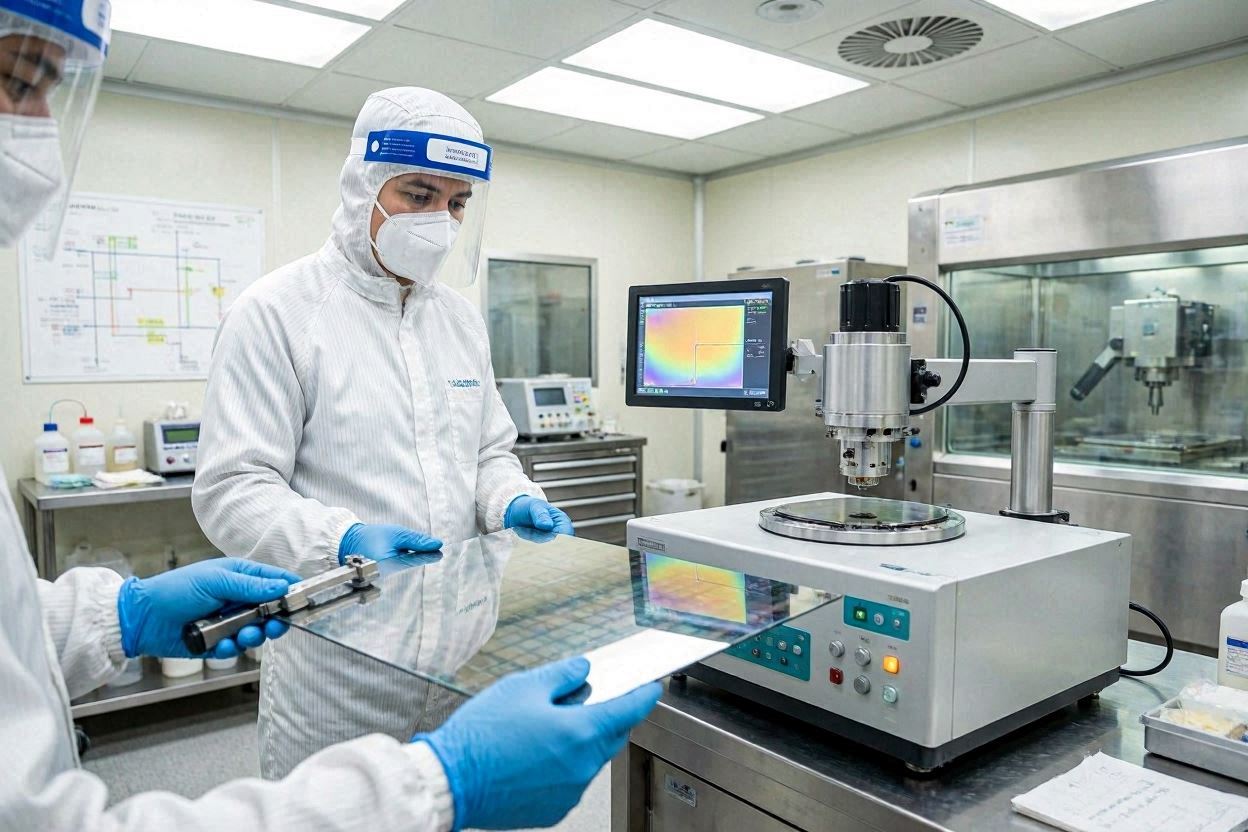
Pad conditioning is one of the most critical and often underappreciated aspects of CMP process control. Without continuous conditioning, CMP performance would drift irreversibly over each pad’s lifetime as the polishing surface degrades — and pad-to-pad process reproducibility would be impossible to achieve.
The Pad Glazing Mechanism
During CMP, the mechanical interaction between the wafer surface and pad asperities, combined with slurry particle and film debris accumulation, progressively degrades the pad surface. Polishing by-products (abraded film material, reacted chemical compounds) fill the pad micropores. The surface asperities — the micro-scale protrusions that make the critical contact with the wafer — are flattened and rounded by repeated mechanical contact. The net result is “pad glazing”: the polishing surface becomes smooth, dense, and poorly wetting — completely unable to transport slurry effectively or maintain contact pressure at feature apexes. A glazed pad shows 50–90% reduction in MRR compared to a freshly conditioned pad, and severely degraded WIWNU.
Diamond Conditioning Disk Operation
The conditioning disk — a stainless steel or titanium disc (4–6 inch diameter) with CVD-deposited synthetic diamond crystals (300–500 µm average protrusion height) distributed across its lower surface — is pressed against the rotating pad surface with controlled force (typically 1–8 lbs) while the disk sweeps back and forth across the pad radius. The diamond crystals abrade the top surface of the pad, removing the glazed layer and re-exposing the fresh open-pore microstructure below. The reconstituted surface has a defined population of sharp asperities that efficiently contact the wafer and transport slurry — restoring the pad to its specification MRR and WIWNU performance.
原位置コンディショニングと原位置コンディショニング
- In-situ conditioning: The conditioning disk operates simultaneously with wafer polishing — while the wafer is on the pad. Maintains nearly constant pad state throughout the polishing run. Requires careful optimization of conditioning force and sweep rate to avoid pad wear that is faster than the desired pad lifetime. Standard for processes where run-to-run MRR stability is the top priority.
- 現場でのコンディショニング: The conditioning disk operates between wafers (no wafer on pad). Allows independent optimization of conditioning parameters without the constraint of not damaging the wafer. Results in some MRR drift between successive wafer polishing runs. Often used in combination with in-situ conditioning.
Conditioning Parameters and Their Effects
| Conditioning Parameter | Higher Value Effect | Lower Value Effect |
|---|---|---|
| Conditioning disk force (lbs) | Faster pad surface refresh; higher pad wear rate; potentially rougher pad texture | Slower pad wear; risk of glazing if too low; more stable pad properties |
| Conditioning sweep speed (mm/s) | More uniform conditioning across pad radius; lower dwell time per zone | Higher dwell time; may create center-heavy conditioning and pad texture gradient |
| Conditioning disk speed (rpm) | Higher diamond coverage per sweep; more uniform diamond wear | Lower coverage; risk of ring patterns on pad surface |
| Conditioning duty cycle (%) | Maintains fresher pad state; higher pad wear rate; more slurry dilution | Lower pad consumption; allows some glazing between conditioning intervals |
07Pad Wear, Lifetime, and End-of-Life Criteria
Polishing pads wear continuously during CMP — both from the mechanical interaction with the wafer surface and from the abrasion of the conditioning disk. The thickness of the top layer decreases over the pad’s useful life, and when the grooves become too shallow (groove depth depleted) or the pad surface properties change sufficiently to cause systematic WIWNU degradation, the pad reaches end-of-life and must be replaced.
Pad Lifetime Drivers
- Conditioning aggressiveness: The conditioning disk removes material from the pad surface with each sweep. Higher conditioning force and duty cycle accelerate pad wear. The pad wear rate must be balanced against the need to maintain fresh surface properties.
- Polishing process: Hard film polishing (tungsten, SiC) causes faster mechanical pad wear than soft film polishing (copper buff). High-pressure recipes accelerate wear relative to low-pressure gentle-buff applications.
- Pad material: Higher-durometer polyurethane pads wear more slowly but may require more aggressive conditioning to maintain surface texture.
End-of-Life Indicators
Pad end-of-life is typically determined by monitoring: (1) pad thickness (laser profilometry or contact gauge), with replacement when the top layer reaches a minimum groove depth threshold (typically when groove depth falls below 60% of initial specification); (2) systematic WIWNU drift that cannot be corrected by conditioning parameter adjustment; or (3) fixed-usage lifetime (total polished wafer count or total polishing time) established during pad qualification. Some advanced fabs implement real-time pad surface health monitoring using in-situ optical profilometry or acoustic emission sensors to detect pad degradation before it impacts wafer yield.
08Fixed Abrasive Pads
Fixed abrasive pads represent an alternative pad architecture where the abrasive particles — typically CeO₂ or Al₂O₃ — are permanently embedded in the pad matrix in a controlled, uniform distribution, rather than being delivered as a separate slurry. These pads are used in conjunction with a slurry-free or minimal-chemistry liquid (an “enabling fluid”) that provides the chemical component of CMP without the abrasive particles.
The primary advantage of fixed abrasive pads is dramatically reduced particle defect density: because the abrasive particles are fixed in the matrix, they cannot form large agglomerates that would scratch the wafer surface. This makes fixed abrasive pads the preferred choice for: post-STI silicon surface finishing (where scratch-free silicon is required before gate oxide growth); advanced copper CMP buff steps; and hybrid bonding surface preparation (where Ra < 0.3 nm and zero scratches are mandatory for void-free bond formation).
The limitation of fixed abrasive pads is their lower MRR compared to free-abrasive slurry (abrasive replenishment is limited by the fixed particle density in the pad matrix), faster pad wear rate (abrasive particles are consumed with each use), and higher unit cost. They are therefore used selectively for applications where defect performance, not throughput, is the primary optimization target.
09Pad Selection Guide by CMP Application
| CMP Application | Recommended Pad Type | 硬度(ショアD) | グルーヴ・パターン | Key Selection Criteria |
|---|---|---|---|---|
| Oxide ILD CMP | Two-layer: hard top + soft sub | 55–65 (top) | Concentric or X-Y grid | Global planarization, WIWNU <2%, low oxide loss rate |
| STI CMP | Two-layer: hard top + soft sub | 55–62 (top) | X-Y grid or spiral | Global planarity, compatible with ceria slurry, low nitride loss |
| タングステンCMP | Two-layer: hard top + soft sub | 58–65 (top) | X-Y grid | Acid resistance (pH 2–4), plug dishing control, high MRR |
| 銅 CMP ステップ 1 | Two-layer: hard top + soft sub | 52–60 (top) | Spiral or X-Y grid | Cu MRR, barrier selectivity, low dishing |
| Cu CMP Barrier/Buff | Single soft or fixed abrasive | 30–45 | Fine grid or smooth | Low scratching, low dishing, barrier clearance, Ra <0.5 nm |
| Hybrid Bonding Prep | Fixed abrasive or ultra-soft | 25–40 | Fine grid or smooth | Ra <0.3 nm, zero scratches, Cu step <2 nm |
| SiC CMP | Hard pad + specialized chemistry | 60–70 | X-Y grid | Chemical resistance to Fenton chemistry, sustained MRR |
10JEEZ CMP Polishing Pads
JEEZ (Jizhi Electronic Technology Co., Ltd.) manufactures CMP polishing pads engineered for the full spectrum of semiconductor planarization applications. As a direct manufacturer, JEEZ produces pads in both single-layer and two-layer stacked configurations, covering oxide ILD, STI, tungsten plug, and copper CMP applications. All JEEZ pads are manufactured from high-purity polyurethane foam with controlled micropore structure, precision-machined groove patterns (X-Y grid, concentric, and spiral variants), and pressure-sensitive adhesive for platen mounting.
JEEZ pad products are validated for chemical compatibility with the full range of JEEZ CMP slurry products, and process qualification data — including MRR, WIWNU, conditioning protocol recommendations, and pad lifetime benchmarks — is available from JEEZ application engineering teams for major CMP tool platforms. JEEZ also supplies absorption and backing films for carrier head assemblies, completing the full consumable package for CMP tool operation.
Get Technical Specifications for JEEZ CMP Polishing Pads
Contact JEEZ to request pad datasheets, conditioning protocol recommendations, or to discuss pad qualification for your specific CMP module and tool platform.
Contact JEEZ →