Post-CMP Cleaning:Methods, Challenges & Best Practices
A complete technical guide to post-CMP wafer cleaning — covering contamination types, brush scrub and megasonic methods, cleaning chemistry selection, metallic contamination control, advanced-node challenges, and best practices for achieving production-ready particle and metal cleanliness specifications.
Why Post-CMP Cleaning Is Critical
Post-CMP cleaning is the final gatekeeping step of the CMP module — and arguably the most consequential for yield. A wafer that has been polished to perfect thickness and planarity can still fail at the next process step if it carries residual slurry particles, metallic contaminants, or organic residues onto the next tool. Unlike many semiconductor process steps, the consequences of inadequate post-CMP cleaning are often invisible at inspection but manifest as reliability failures, leakage current, or catastrophic yield loss at end-of-line electrical test.
Post-CMP cleaning is an integral part of the CMP module, not a separate step, and must be optimised in conjunction with the slurry chemistry and polishing process. For the full context of where cleaning fits within the CMP workflow, see the CMP Semiconductor Complete Guide and our CMP Process Step-by-Step の記事を参照されたい。.
Contamination Types After CMP
Understanding the nature of each contaminant type on the post-CMP wafer surface is the foundation for designing an effective cleaning process. The four major contamination categories have distinct chemical and physical characteristics that require different removal mechanisms.
Particulate Contamination
Residual slurry abrasive particles (silica, ceria, alumina) and polishing by-product particles adhering to the wafer surface by van der Waals and electrostatic forces.
Metallic Contamination
Dissolved metal ions (Cu²⁺, Fe³⁺, Ce³⁺/Ce⁴⁺) adsorbed on oxide and silicon surfaces. Copper is especially damaging — it diffuses through SiO₂ and poisons transistor junctions.
Organic Contamination
Slurry additives (surfactants, BTA corrosion inhibitor, chelating agents) and dissolved carbon species adsorbed on the surface. These can block subsequent deposition reactions.
Chemical Residues
pH-adjusted residual reaction by-products and oxidiser decomposition products that alter surface chemistry and can cause local corrosion or adhesion failures.
Particle Adhesion Forces
Slurry particles adhere to the wafer surface through a combination of van der Waals attraction, electrostatic interaction, and — once dried — capillary and chemical bonding. The magnitude of the adhesion force is particle-size-dependent: smaller particles (sub-100 nm) have a higher surface-area-to-mass ratio and adhere more tenaciously per unit mass, making them harder to remove by mechanical scrubbing alone.
The key insight for designing an effective particle removal process comes from zeta potential theory: if the surface charge (zeta potential) of the particle and the wafer surface are of the same sign and sufficiently large in magnitude, electrostatic repulsion will prevent re-adhesion of particles that have been dislodged from the surface. Cleaning chemistry is therefore formulated to simultaneously dislodge particles (through chemical dissolution of the surface monolayer or mechanical brush action) and maintain like-charge repulsion between the dislodged particles and the clean surface.
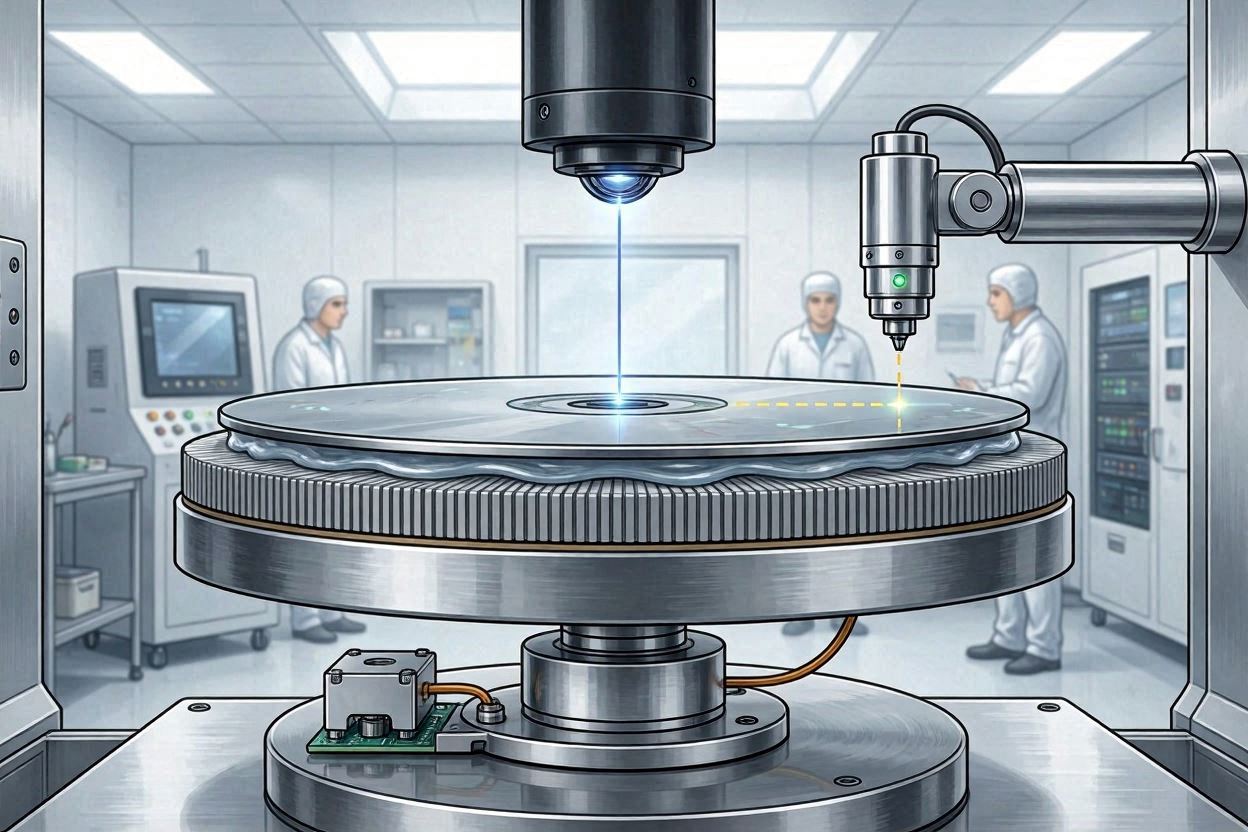
Standard Post-CMP Cleaning Sequence
The standard post-CMP cleaning sequence in a production fab consists of four stages performed in an integrated cleaning module immediately following polishing.
-
1
Initial Rinse (Bulk Slurry Removal)
The wafer is immediately rinsed with high-flow deionised water (DIW) to dilute and displace the bulk slurry film. This step reduces the particle load on the surface by 90–95% and prevents slurry from drying on the wafer. Some tools use a DI water spray at the polishing station before the wafer is transferred to the cleaning module.
-
2
Primary Brush Scrub with Chemical Dispense
Rotating PVA (polyvinyl alcohol) sponge brushes contact both sides of the wafer while cleaning chemistry is dispensed. The brushes provide mechanical scrubbing force to dislodge remaining particles and the cleaning chemistry maintains the electrostatic environment to prevent re-adhesion. This is the primary particle and organic removal step. Duration: typically 20–60 seconds per side.
-
3
Secondary Rinse and Optional Second Scrub
A DIW rinse removes the cleaning chemistry and displaced contaminants. For demanding applications (metal CMP, advanced nodes), a second brush scrub with different chemistry targeting metallic contamination may follow. This second step typically uses dilute HCl or citric acid to complex and remove surface metal ions.
-
4
Spin-Rinse-Dry (SRD)
The wafer is spun at high speed (1,500–3,000 RPM) while DIW is dispensed, then the water supply is cut and the wafer spins dry under a nitrogen or IPA vapour atmosphere. The drying step is critical: watermarks (dried DIW residue containing trace mineral ions) must be avoided. IPA vapour-assisted drying significantly reduces watermark formation by lowering surface tension at the receding water front.
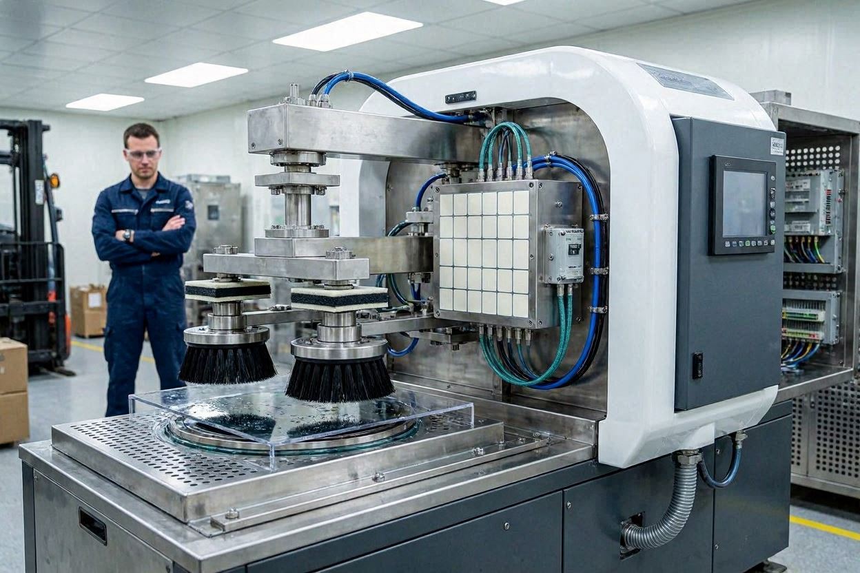
Brush Scrub Cleaning: Mechanics and Variables
Brush scrub cleaning is the backbone of post-CMP particle removal. The PVA brush — a highly porous, hydrophilic sponge with a surface texture of fine nodules — contacts the wafer surface and removes particles through a combination of direct mechanical displacement, hydrodynamic fluid shear, and electrostatic management via the dispensed cleaning chemistry.
Brush Contact Mode and Pressure
The brush must make light, controlled contact with the wafer surface — enough to generate the shear force needed to dislodge particles but not so much that it introduces new scratches from abrasive material embedded in the brush. Optimal brush contact force is typically 0.02–0.1 N/cm². The brush is pre-soaked in DIW before use to ensure full swelling of the PVA foam structure; a dry or partially dried brush will scratch the wafer surface.
Cleaning Chemistry Dispense
The cleaning chemistry must be dispensed onto the brush-wafer interface continuously during scrubbing. The dispense chemistry serves multiple functions: adjusting surface zeta potential to promote particle repulsion, chemically dissolving surface oxide monolayers to expose trapped particles, complexing metal ion contaminants for removal, and lubricating the brush-wafer interface to reduce mechanical friction.
Brush Lifetime Management
PVA brushes have a finite lifetime — typically 500–2,000 wafer passes depending on the slurry type and CMP application. A worn or contaminated brush loses its cleaning effectiveness and can become a source of contamination itself as accumulated particles are re-deposited. Brush monitoring (via optical inspection or electrical resistance measurement) and regular replacement are essential elements of post-CMP cleaning process control.
Megasonic Cleaning
Megasonic cleaning uses high-frequency acoustic energy (800 kHz–1 MHz) transmitted through a liquid bath or liquid film on the wafer surface to remove sub-100 nm particles that brush scrubbing cannot dislodge. It is particularly valuable for post-CMP cleaning at advanced nodes where feature sizes are below 10 nm and conventional brush contact forces risk damaging fragile structures.
Acoustic Streaming Mechanism
At megasonic frequencies, acoustic pressure waves create two simultaneous effects: acoustic streaming (bulk fluid motion that transports contaminants away from the surface) and micro-cavitation (formation and collapse of microscopic bubbles near particle surfaces, generating localised impulsive forces that dislodge adhering particles). Unlike ultrasonic cleaning at lower frequencies (20–100 kHz), megasonic cleaning at 800 kHz–1 MHz uses much smaller bubble formation events that generate sufficient force to remove sub-100 nm particles without damaging fragile silicon nanosheet or low-k dielectric structures.
Application Considerations
The effectiveness of megasonic cleaning depends critically on the transducer frequency, power density, and the chemistry of the liquid medium. Megasonic cleaning is most effective in alkaline solutions (where particle and surface zeta potentials are both negative) and loses effectiveness in near-neutral or acidic environments. For copper CMP post-clean, where acidic chemistry is preferred to remove copper ions, a sequential approach is used: first an acidic brush scrub for metal removal, then a megasonic step in alkaline chemistry for particle removal.
Cleaning Chemistry by Surface Type
| Surface / CMP Type | Primary Chemistry | pH範囲 | Target Contaminants | Key Considerations |
|---|---|---|---|---|
| Oxide / STI post-clean | Dilute NH₄OH + surfactant | 9-11 | Ceria / silica particles, organics | High pH promotes electrostatic particle repulsion; minimize silicon etch |
| Copper post-clean (bulk) | Dilute citric acid or HCl + surfactant | 2-5 | Cu ions, BTA residues, slurry particles | Acidic pH dissolves Cu oxide; BTA removal requires surfactant or oxidative rinse |
| Copper post-clean (barrier step) | Dilute HCl + corrosion inhibitor | 2-4 | Residual TaN/Ta particles, Cu ions | Avoid over-etching exposed low-k dielectric; use inhibitor to protect Cu |
| Tungsten post-clean | Dilute HF or HCl + chelating agent | 2-4 | Alumina particles, Fe ions, W residues | HF dissolves native oxide to release trapped particles; handle with extreme caution |
| Low-k dielectric post-clean | Neutral pH organic solvent blend | 6–8 | Slurry particles, organic residues | Avoid aggressive chemistry that absorbs into porous low-k; delamination risk |
Metallic Contamination Control
Metallic contamination on silicon surfaces is among the most insidious yield-killers in semiconductor manufacturing. Of all the metals encountered in CMP — iron from slurry oxidizers, cerium from ceria abrasives, tungsten from W CMP — copper is the most dangerous and receives the most engineering attention.
Why Copper Contamination Is So Harmful
Copper is a deep-level trap in silicon: it introduces energy states near the middle of the silicon bandgap that dramatically increase minority carrier recombination, degrade gate oxide reliability, and increase junction leakage current. Critically, copper diffuses through silicon dioxide far more rapidly than any other common metal — at the temperatures encountered in downstream thermal steps (200–400°C), copper can traverse a 10 nm SiO₂ gate dielectric in milliseconds.
For FEOL applications, the copper surface contamination budget is typically <1×10¹⁰ atoms/cm² — a level requiring extremely sensitive measurement (total reflection X-ray fluorescence, TXRF) and carefully designed cleaning chemistry. Post-CMP cleaning sequences for copper involve a dedicated metallic contamination removal step using dilute hydrochloric acid (HCl) or organic chelating agents (citric acid, EDTA) to complex dissolved copper ions and remove them from the surface into solution for subsequent rinsing.
Cerium and Iron Contamination
Cerium ions from ceria slurries and iron ions from ferric-nitrate-based tungsten slurries are both capable of forming insoluble surface precipitates that resist standard water rinsing. Dilute acid cleaning (HCl, HF) is effective at dissolving these metal hydroxide deposits. Cerium contamination is particularly challenging because CeO₂ particles can chemically bond to silicon oxide surfaces through Ce–O–Si linkages that are only broken by acidic conditions.
Advanced-Node Cleaning Challenges
As device dimensions shrink below 5 nm and 3D architectures such as GAA and hybrid bonding become mainstream, post-CMP cleaning faces challenges that existing production processes cannot fully address.
- Sub-10 nm particle removal: Particles below 10 nm adhere with forces proportionally much larger relative to their mass than larger particles. Megasonic energy levels required to remove these particles approach thresholds that damage fragile nanosheet structures, creating a fundamental tension between cleaning effectiveness and device integrity.
- Low-k dielectric compatibility: Porous ultra-low-k dielectrics (k < 2.2) are chemically and mechanically fragile — aggressive cleaning chemistry or brush contact can cause pore collapse, carbon depletion, or delamination. Cleaning chemistry for low-k applications must be specifically formulated to avoid moisture absorption into the dielectric pore network.
- Cobalt corrosion during cleaning: As cobalt replaces tungsten in local interconnects at 5 nm and below, post-CMP cleaning must carefully manage cobalt corrosion. Cobalt dissolves readily in both acidic and alkaline solutions; the cleaning pH window where cobalt is stable is very narrow (approximately pH 8–9). This conflicts with the broader pH ranges used for particle and metal removal, requiring innovative cleaning sequence designs.
- Hybrid bonding surface preparation: For hybrid bonding applications, the post-CMP surface must achieve roughness below 0.3 nm Ra and a metal ion concentration below the detection limit of most characterisation tools. This requires a final “super-clean” step — often a dilute SC-1 (NH₄OH/H₂O₂/H₂O) clean followed by a thorough DIW rinse and IPA-assisted drying.
For broader context on CMP challenges at advanced nodes, see our article: CMP in Advanced Nodes: Challenges at 7nm, 5nm & Beyond.
Best Practices Checklist
Post-CMP Cleaning Best Practices
1. Never allow the wafer to dry before the first rinse. Transfer from polish to first wet contact must be under 30 seconds.
2. Match cleaning chemistry pH to target contamination type and surface material. Alkaline for oxide particle removal; acidic for metal ion removal.
3. Monitor brush condition on a scheduled interval. Replace before wear causes cleaning effectiveness to degrade or re-contamination to occur.
4. Use IPA-assisted or IPA-vapour drying to prevent watermarks on device surfaces.
5. Validate DI water quality regularly (TOC <1 ppb, resistivity 18.2 MΩ·cm, particle count <1/mL >50 nm).
6. Include a dedicated metallic removal step for copper and metal CMP. Verify surface metal levels by TXRF on a monitor wafer after cleaning qualification.
7. Perform cleaning efficiency verification (particle removal efficiency, PRE) after any change to cleaning chemistry, flow rate, brush, or process time.
CMP Consumables for Production Environments
JEEZ supplies CMP slurries and polishing pads to fabs worldwide. Our technical team is ready to support your process qualification and optimisation needs.
Contact JEEZ →