What Is CMP Slurry? A Complete Guide to Chemical Mechanical Planarization
Everything you need to know about CMP slurry — from fundamental chemistry and process mechanics to formulation science and real-world semiconductor manufacturing applications.
Chemical mechanical planarization — CMP — is one of the most widely used and process-critical techniques in modern semiconductor manufacturing. Yet despite its ubiquity, the consumable at the heart of every CMP process, the CMPスラリー, remains poorly understood outside of the specialist engineering community. This guide explains what CMP slurry is, how it works, what it is made of, and why selecting the right formulation for each application is one of the highest-leverage decisions a process engineer can make.
1. Defining CMP and CMP Slurry
化学的機械的平坦化(CMP) is a semiconductor wafer processing technique that uses the simultaneous action of chemical reactions and mechanical abrasion to remove material from a wafer surface and achieve a flat, smooth, and globally planar result. It is the only technique currently capable of achieving the sub-nanometer surface uniformity required for multi-layer device fabrication at advanced technology nodes.
CMPスラリー is the engineered aqueous suspension that enables this process. It is dispensed between a rotating polishing pad and the wafer surface during CMP, acting as the reactive, abrasive medium that drives material removal. Without a carefully formulated slurry, the pad alone cannot achieve the removal rates, selectivity, or surface quality that modern device integration demands.
A CMP slurry is not a simple abrasive paste. It is a precision chemical system in which abrasive particles, oxidizing agents, pH buffers, chelating agents, corrosion inhibitors, and surfactants work in concert to deliver controlled, repeatable, and highly selective material removal at atomic-scale precision.
Key distinction: CMP is fundamentally different from dry plasma etching. Plasma etch is anisotropic — it removes material directionally, in patterns defined by a lithographic mask. CMP is isotropic and maskless — it acts on the entire wafer surface simultaneously, preferentially removing the highest topographic points to achieve global planarity. These two processes are complementary, not competitive.
2. Why CMP Is Indispensable in Semiconductor Fabrication
As integrated circuit designs have evolved from single-layer devices to multi-layer three-dimensional structures with dozens of stacked metal and dielectric layers, the requirement for precise inter-layer planarity has become non-negotiable. Each layer deposited on a non-planar surface inherits and amplifies the topography of the layer below. Without periodic planarization, cumulative surface roughness would make photolithographic patterning of subsequent layers impossible — the depth of focus of advanced lithography tools is measured in nanometers, far less than the topographic variation that would accumulate without CMP.
CMP solves this problem by resetting the surface to near-perfect flatness after each key deposition step. Modern logic devices may undergo 15 to 25 separate CMP steps across their full fabrication flow, each targeting a different film material and each requiring a different slurry chemistry.
Beyond planarity, CMP is also used for material removal in damascene metal patterning — the process by which copper interconnects are formed by depositing metal into pre-etched trenches and then polishing away the excess, leaving metal only in the intended conductor paths. This application places extremely demanding requirements on CMP slurry performance, particularly in controlling dishing (over-polish of wide metal features) and erosion (removal of dielectric between metal lines).
3.CMPプロセスの仕組み
face-down
on pad surface
material removal
detection
clean & inspect
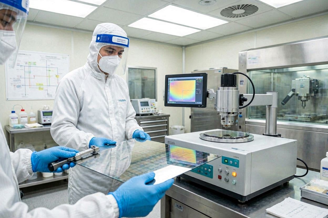
In a typical CMP tool (also called a polisher), the wafer is held face-down in a carrier head that applies controlled downforce against a rotating polishing pad mounted on a platen. Slurry is continuously dispensed onto the pad surface at a controlled flow rate. The combined rotation of the carrier head and platen, along with the lateral sweep of the carrier, distributes slurry across the wafer surface and drives the material removal process through two simultaneous mechanisms:
- Chemical action: The liquid phase of the slurry — oxidizers, acids, and chelating agents — reacts with the target film material, transforming the hard surface into a softer, more easily abraded chemical product. For copper CMP, hydrogen peroxide oxidizes the copper surface to copper oxide, which is far more mechanically compliant than metallic copper. For oxide CMP with ceria abrasives, a direct Si–O–Ce bond forms at the slurry-wafer interface, enabling a chemical tooth-and-pull removal mechanism.
- Mechanical action: Abrasive particles suspended in the slurry impact and abrade the chemically weakened surface, physically removing material. The hardness, size, concentration, and shape of these particles — along with the applied downforce and relative velocity — determine the mechanical component of the removal rate.
The interplay between these two mechanisms is where CMP slurry science becomes genuinely complex. Optimizing one without disturbing the other requires deep knowledge of surface chemistry, tribology, and fluid dynamics simultaneously.
4. CMP Slurry Composition: What Is Inside the Bottle
Ceria, colloidal silica, or alumina. Drive mechanical removal. Size typically 20–200 nm.
H₂O₂, KIO₃, or Fe(NO₃)₃. Reacts with target film to form a softer, removable product.
Acids, bases, or buffering salts. Controls solution acidity, which governs reaction kinetics.
Organic acids (citric, oxalic, glycine). Complexes dissolved metal ions and aids removal.
BTA (benzotriazole) for copper slurries. Forms passivation film to control corrosion rate.
Keeps abrasive particles stable and well-dispersed. Prevents agglomeration and LPC.
Ultra-pure deionized water as the continuous phase. Typically 85–95% of total volume.
Each of these components interacts with every other. Changing the oxidizer concentration affects the corrosion inhibitor’s effectiveness. Adjusting pH shifts the zeta potential of the abrasive particles, which changes their dispersion stability and can affect removal rate dramatically. This interdependence is why CMP slurry development is genuinely difficult and why formulation expertise — accumulated over years of process integration experience — is the primary differentiator between slurry manufacturers.
JEEZ develops each slurry formulation as a complete system, optimizing all components simultaneously rather than treating them as independent variables. This systems approach is particularly important for demanding applications such as wide-bandgap semiconductor polishing and advanced packaging CMP, where standard formulations frequently fall short.
5. Abrasive Particle Types and Their Roles
The abrasive is the most visible component of a CMP slurry and, in many ways, the most consequential. Three abrasive materials dominate the industry:
セリア
Ceria is the abrasive of choice for oxide and STI (Shallow Trench Isolation) CMP applications. Its unique advantage lies in a chemical removal mechanism — cerium ions at the abrasive surface form direct Ce–O–Si bonds with the silicon dioxide surface, enabling a “chemical tooth-and-pull” effect that delivers very high removal rates (often 2,000–5,000 Å/min on thermal oxide) with excellent selectivity over silicon nitride. This selectivity is critical in STI CMP, where over-polishing through the nitride stop layer would destroy device structures.
コロイダルシリカ(SiO₂)
Colloidal silica particles — synthesized by controlled hydrolysis of silicate precursors to yield uniformly spherical, monosize particles — are the premier choice where surface finish is paramount. Their relatively low hardness (Mohs ~7) and smooth, spherical morphology produce gentle, uniform material removal with minimal subsurface damage. Silicon wafer final polishing, copper CMP, and precision low-k dielectric planarization all rely on colloidal silica. Surface roughness values below 0.05 nm Ra are achievable on silicon with optimized colloidal silica slurries.
アルミナ(Al₂O₃)
Alumina’s high hardness (Mohs 9) makes it the standard abrasive for tungsten CMP, where the target film — tungsten metal or its oxide WO₃ — requires aggressive mechanical abrasion at low pH (typically 2–4) with hydrogen peroxide as the oxidizer. Alumina slurries deliver removal rates of 100–400 nm/min on tungsten under optimized conditions. The trade-off is higher scratch risk and surface roughness compared to silica-based systems, which must be managed through particle size selection and process optimization.
For a detailed technical comparison of all three abrasive types, including selection criteria and performance trade-offs, see our dedicated article: CMP Slurry Abrasives Explained: Silica vs Alumina vs Ceria.
6. Key Performance Metrics for CMP Slurry
| メートル | Definition | 代表的な仕様 | なぜ重要なのか |
|---|---|---|---|
| MRR | Material Removal Rate | 100–5,000 Å/min (varies by film) | Determines throughput and process time |
| 選択性 | MRR ratio between target and stop films | 10:1 to >100:1 (oxide:nitride for STI) | Controls when polishing stops at intended layer |
| WiWNU | Within-Wafer Non-Uniformity | <3% (1σ) for production processes | Determines yield uniformity across the wafer |
| LPC | Large Particle Count (>1 µm) | <50 particles/mL (typical spec) | Large particles are the primary scratch defect source |
| Zeta Potential | Surface charge of abrasive particles | |±30 mV| minimum for stability | Low zeta potential leads to agglomeration and defects |
| pH | Acidity/alkalinity of slurry | 2–4 (W), 7–9 (Cu), 10–11 (oxide) | Governs reaction kinetics and particle stability |
| Dishing / Erosion | Over-polish of metal/dielectric features | <20 nm dishing for Cu lines (advanced node) | Affects electrical resistance and signal integrity |
Understanding and specifying these metrics correctly is the first step in any slurry qualification program. Engineers who focus only on MRR often discover that a high-removal-rate slurry introduces unacceptable defect density or dishing — reinforcing the need to treat slurry performance as a multi-dimensional optimization problem.
7. CMP Slurry vs CMP Pad: How They Work Together
CMP slurry and the polishing pad are the two primary consumables in any CMP process, and their interaction is inseparable. The pad’s surface texture — its asperities, grooves, and hardness — determines how slurry is distributed across the wafer, how uniformly abrasive particles contact the surface, and how effectively the reaction products and polished material are swept away from the interface.
A slurry optimized for one pad type may perform very differently on a different pad. This is why leading CMP consumable manufacturers — including JEEZ — characterize their slurries across multiple pad types and provide guidance on pad-slurry pairing as part of their application engineering support. Matching slurry chemistry to pad mechanics is one of the most impactful levers available to process engineers seeking to improve planarization performance without changing the tool or film stack.
Application note: Pad conditioning — the process of refreshing the pad surface with a diamond conditioner disk during CMP — also interacts strongly with slurry performance. Over-conditioning opens the pad surface and increases MRR but can also increase surface roughness. Under-conditioning glazes the pad and reduces slurry transport, causing MRR drift over time. Establishing the optimal conditioning recipe is a key part of slurry process development.
8. Where CMP Slurry Is Used in the Fab
CMP is not a single process step — it is a family of related processes used at multiple points throughout the device fabrication flow. Each application has its own slurry requirements:
- Shallow Trench Isolation (STI) CMP: Removes oxide overfill after trench filling, stopping on nitride. Ceria slurries with high oxide:nitride selectivity are the standard. This is one of the earliest CMP steps in the FEOL flow.
- Inter-Layer Dielectric (ILD) CMP: Planarizes oxide or low-k dielectric layers between metal interconnect levels. Ceria or silica slurries depending on the dielectric material and required surface finish.
- タングステン(W) CMP: Removes tungsten overfill from via and contact fill steps. Alumina slurries at low pH with peroxide oxidizer. Critical for contact resistance control.
- 銅(Cu)CMP: Three-stage process — bulk Cu removal, copper clearing, and barrier metal removal. Different slurry formulations for each stage. The most chemically complex CMP application in mainstream logic and memory devices.
- Silicon Wafer Polishing: Final polishing of bare silicon substrates to achieve epi-ready surfaces. Colloidal silica slurries at high pH (10–11). Surface roughness is the primary quality metric.
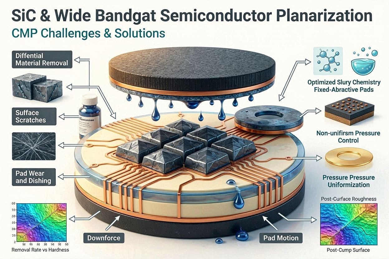
- SiC and Wide-Bandgap Substrate Polishing: Highly demanding due to material hardness. Specialized slurry formulations with advanced abrasive systems. A growing application driven by EV and power electronics demand. See: CMP Slurry for SiC Wafer Polishing: Challenges & Solutions.
- Advanced Packaging CMP: TSV reveal, RDL planarization, hybrid bonding surface preparation. Emerging and rapidly evolving application area. See: Advanced Packaging CMP: Slurry Requirements for 3D NAND & TSV Processes.
For a complete technical breakdown of each slurry type, including formulation chemistry and process parameter ranges, see our comprehensive article: CMPスラリーの種類酸化物、STI、銅、タングステン、その他.
9. Selecting the Right CMP Slurry
Given the diversity of CMP applications and the complexity of slurry formulation science, there is no universal “best” CMP slurry. Selection must be driven by the specific film system being polished, the process integration constraints, the tool and pad configuration, and the target performance specifications for removal rate, selectivity, defectivity, and planarization efficiency.
The slurry manufacturer’s role extends well beyond supplying a chemical. JEEZ’s application engineering team provides full process integration support — from initial formulation selection and parameter optimization through qualification, production ramp, and ongoing process monitoring. This partnership model is particularly valuable for customers working with non-standard materials, tight process windows, or new integration schemes where published data is limited.
For a structured, step-by-step approach to slurry selection from a process engineering perspective, see our dedicated selection guide: How to Choose a CMP Slurry: Selection Guide for Semiconductor Engineers. For an overview of the leading global manufacturers and their product portfolios, see: Top CMP Slurry Manufacturers: Global Supplier Guide 2026.
Have Questions About CMP Slurry for Your Process?
JEEZ’s application engineers specialize in matching slurry formulations to process requirements — from mainstream oxide and copper CMP to demanding SiC and advanced packaging applications. Reach out for a no-obligation technical consultation.
Contact Our Experts →