地子電子の最新動向、重要なお知らせ、企業ニュースなどをお知らせします。当社の成長の軌跡と重要なマイルストーンをお客様と共有することをお約束します。.
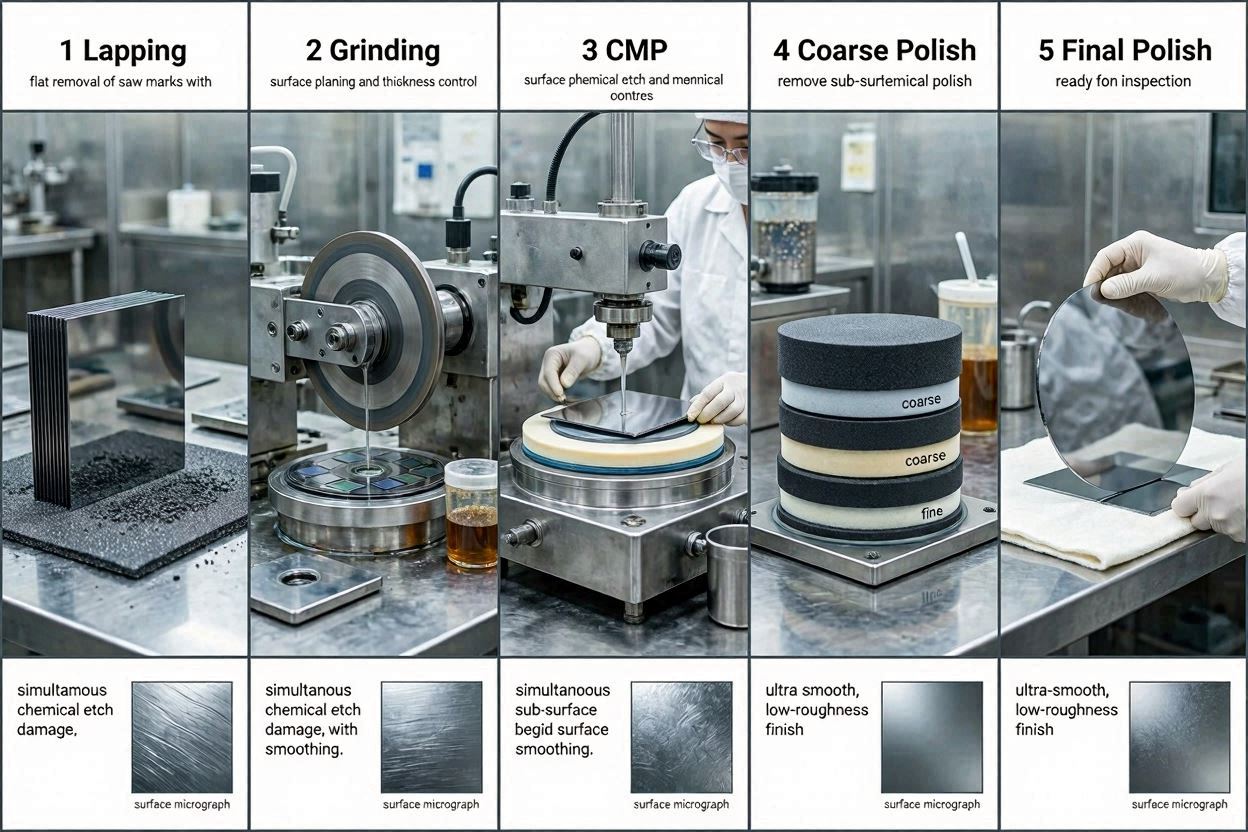
← Back to: The Complete Guide to Silicon Wafer Polishing JEEZ Semiconductor Materials · Technical Guide · Updated June 2026 A detailed technical walkthrough of every stage in the silicon ...
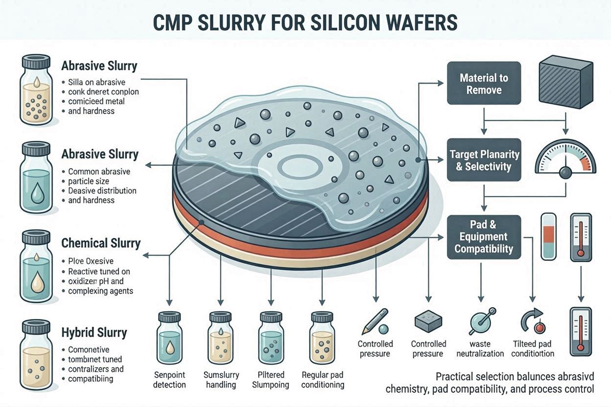
← Back to: The Complete Guide to Silicon Wafer Polishing JEEZ Semiconductor Materials · Technical Guide · Updated June 2026 A complete engineer’s guide to colloidal silica, fumed silica, and ...
JEEZ Semiconductor Materials · Technical Deep-Dive · Updated June 2026 From the physics of chemical-mechanical planarization to slurry formulation, defect management, and cost control — the definitive reference for process ...
JEEZ · Applications CMP Slurry for Advanced Packaging and TSV Advanced packaging and through-silicon vias have made CMP critical to the back end as well as the front end. This ...
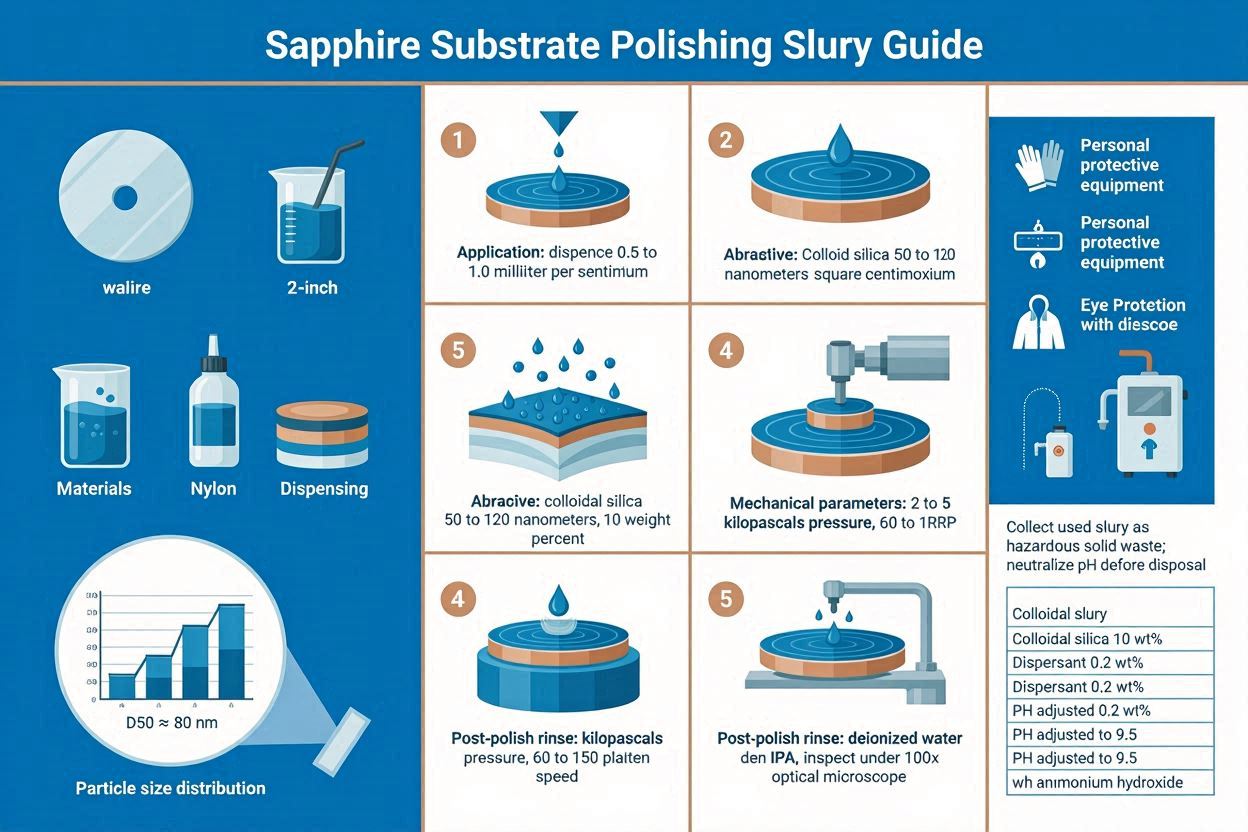
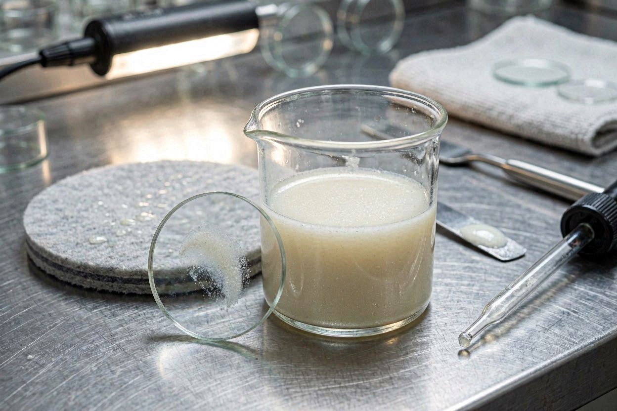
JEEZ · Applications Sapphire is one of the hardest substrates in production, used for LED, optical and specialty semiconductor applications. This guide explains how sapphire substrate polishing slurry works — ...
JEEZ · Applications Precision optics demand surfaces measured in nanometres of roughness and fractions of a wavelength of figure. This guide explains how polishing slurry works for optical glass and ...

JEEZ · Sourcing & Procurement Bringing a new slurry vendor online protects a production line only if it is done rigorously. This guide is a step-by-step checklist for qualifying a ...
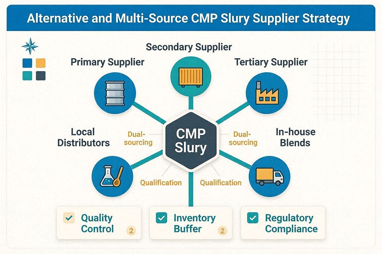
JEEZ · Sourcing & Procurement Alternative and Multi-Source CMP Slurry Supplier Strategy Market consolidation has made single-source slurry supply riskier than ever. This guide explains how to build a multi-source ...
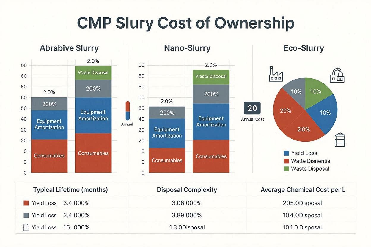
JEEZ · Sourcing & Procurement The price per litre is one of the least useful numbers when comparing CMP slurries. This guide explains total cost of ownership — the consumption, ...
JEEZ · Sourcing & Procurement The CMP slurry supplier landscape has changed sharply by June 2026. This guide explains the types of manufacturers in the market, what genuinely separates them, ...
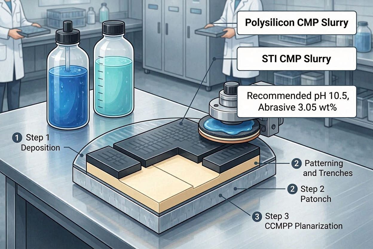
JEEZ · Selection by Material Shallow Trench Isolation and polysilicon steps require carefully balanced selectivity so the process self-terminates at the right depth. This guide explains how to select a ...
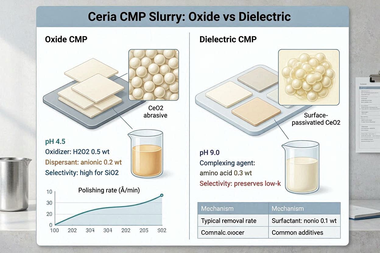
JEEZ · Selection by Material Interlayer dielectric and bulk oxide removal rely heavily on cerium-oxide chemistry. This guide explains how to select an oxide and dielectric CMP slurry — why ...