SiC & Wide Bandgap Semiconductor Planarization: CMP Challenges & Solutions
Silicon carbide, gallium nitride, and other wide bandgap semiconductors are the materials enabling the next generation of power electronics — from electric vehicle inverters to renewable energy converters and industrial motor drives. But these materials’ exceptional physical properties make them among the most challenging substrates to planarize. This guide covers the science of SiC and WBG CMP: why conventional silicon CMP approaches fail, what advanced chemistries are solving the problem, and what the market and technology trends mean for CMP in power semiconductor manufacturing.
01Why Wide Bandgap Materials Need Different CMP
The material properties that make silicon carbide (SiC), gallium nitride (GaN), and related wide bandgap (WBG) semiconductors superior to silicon for high-voltage, high-temperature power device applications — extreme hardness, high chemical stability, wide bandgap, high breakdown electric field — are the same properties that make them extremely difficult to planarize. The materials polished well by alkaline colloidal silica on a standard silicon CMP process tool are soft and chemically reactive. SiC and GaN are neither.
| Недвижимость | Кремний (Si) | Silicon Carbide (4H-SiC) | Нитрид галлия (GaN) | Diamond |
|---|---|---|---|---|
| Mohs Hardness | 6.5 | 9.2–9.5 | 8.5–9.0 | 10 (hardest known) |
| Bandgap (eV) | 1.12 | 3.26 | 3.44 | 5.47 |
| Breakdown Field (MV/cm) | 0.3 | 3.0 | 3.3 | 10 |
| Химическая стойкость | Moderate (KOH etches) | Очень высокий | Высокий | Extreme |
| Typical CMP MRR (nm/min) | 200–500 | 10–100 | 5–50 | <5 |
| Wafer Size (standard, 2026) | 300 mm | 150–200 mm | 150–200 mm (on Si or SiC) | 2–4 inch |
The CMP MRR values illustrate the challenge dramatically: SiC is polished at 10–50× lower rates than silicon under comparable conditions. At commercial SiC wafer polishing throughput requirements (typically 40–80 wafers per hour on a production polishing tool), this MRR disparity directly translates to either longer polishing times (reducing throughput) or higher applied pressures (risking subsurface damage and higher defect density).
02SiC Material Properties and CMP Challenges
Crystal Structure and Polytypes
Silicon carbide exists in over 200 polytypes — different stacking sequences of the same Si and C atomic layers — of which 4H-SiC (hexagonal, 4-layer stacking period) and 6H-SiC (hexagonal, 6-layer) are most relevant for power device manufacturing. 4H-SiC is preferred for power MOSFETs and Schottky diodes because of its superior isotropic electron mobility and larger bandgap relative to 6H-SiC. 3C-SiC (cubic) is used for research applications. The polytype-dependent crystal structure influences CMP behavior through differences in surface bond energy, oxidation rate, and cleavage plane orientation.
Hardness and Its CMP Consequences
With a Mohs hardness of 9.2–9.5, 4H-SiC is harder than all common CMP abrasive materials except diamond (Mohs 10) and is comparable to aluminum oxide (Mohs 9.0). This means that:
- Colloidal silica particles (SiO₂, Mohs 7) are too soft to mechanically scratch SiC surfaces at useful MRR levels under standard CMP pressures
- Fumed alumina (Al₂O₃, Mohs 9.0) is marginally harder than SiC but produces high surface scratch densities due to angular particle morphology
- Diamond abrasive provides the highest MRR but introduces subsurface crystal damage that is unacceptable for epitaxial layer growth quality
- The only practical approach is to chemically soften the SiC surface before mechanical abrasion — the key principle behind all advanced SiC CMP chemistries
Chemical Stability
SiC’s strong Si–C covalent bonds (bond dissociation energy: 451 kJ/mol for Si–C vs. 368 kJ/mol for Si–O) make it resistant to most aqueous chemical etchants at room temperature. Conventional silicon CMP relies on alkaline chemistry (KOH, NH₄OH at pH 10–12) breaking Si–O–Si bonds on the oxidized silicon surface. This mechanism is largely ineffective on SiC because the native SiO₂ that forms on SiC surfaces at room temperature is much thinner (0.5–2 nm vs. 1–4 nm on Si) and grows more slowly, limiting the rate of chemical surface modification that CMP can exploit.
03Si-Face vs. C-Face: The Polarity Problem
A 4H-SiC wafer has two distinct surfaces: the silicon-terminated face (Si-face, crystallographic direction [0001]) and the carbon-terminated face (C-face, [000-1]). These two surfaces have fundamentally different physical and chemical properties that complicate SiC CMP in multi-wafer batch processing:
Si-Face (0001)
The Si-face is the primary device fabrication surface for power MOSFETs and Schottky diodes in 4H-SiC. It oxidizes more slowly than the C-face (oxidation rate ratio ~10:1). Surface roughness after standard polishing is lower. Majority of SiC CMP development targets the Si-face. Target Ra for epi-ready wafers: <0.2 nm.
C-Face (000-1)
The C-face oxidizes significantly faster than the Si-face (10× higher oxidation rate under comparable conditions). This means that under identical CMP conditions, the C-face polishes substantially faster — creating a MRR asymmetry problem in any process that exposes both faces simultaneously. C-face surfaces are also more reactive to CMP slurry chemistry, requiring careful pH and oxidizer concentration control to avoid excessive material removal or roughness.
In single-wafer SiC CMP (which processes only the Si-face at a time), the polarity problem is manageable. In batch-process multi-wafer polishing (which polishes multiple wafers simultaneously in a carrier), wafers with different orientations or with both faces exposed due to carrier design can experience different MRR, leading to thickness non-uniformity within the batch. Production SiC polishing systems must account for this through carrier design, wafer fixturing, and process recipe optimization.
04Why Conventional Silicon CMP Fails for SiC
A conventional silicon CMP process — colloidal silica at pH 10–11, standard polyurethane pad, 2–4 psi down-force — applied directly to a 4H-SiC substrate produces:
- MRR of 1–5 nm/min: Compared to 200–400 nm/min for silicon oxide. At a commercial requirement to remove 10–20 µm of SiC material per wafer (to correct saw damage and subsurface crystal damage from wafer slicing), a 5 nm/min MRR requires 33–67 hours of polishing per wafer — clearly non-viable for any commercial manufacturing operation.
- Surface scratches from hard abrasive particles: At the contact pressures needed to achieve even 5 nm/min MRR on SiC with silica, the abrasive particles cause surface scratching because the silica particle hardness is below SiC hardness — the interaction is dominated by shear and gouging rather than the gentle abrasive cutting that produces smooth silicon surfaces.
- Inadequate surface roughness: Ra after conventional silica CMP on SiC is typically 1–5 nm — an order of magnitude higher than the <0.2 nm Ra required for epi-ready SiC substrates for homoepitaxial SiC layer growth for power device fabrication.
The CMP paradigm for SiC must reverse the usual silicon approach: instead of relying on mechanical abrasion enhanced by mild chemistry, SiC CMP must rely on chemistry to rapidly soften/convert the surface to a more easily abraded compound, with mechanical abrasion as the secondary removal step. This is the key principle behind all successful advanced SiC CMP chemistries.
05Fenton Chemistry for SiC CMP
The Fenton reaction — discovered by H.J.H. Fenton in 1894 — involves the catalytic decomposition of hydrogen peroxide (H₂O₂) by ferrous iron (Fe²⁺) to generate highly reactive hydroxyl radicals (·OH):
Fe²⁺ + H₂O₂ → Fe³⁺ + ·OH + OH⁻
Hydroxyl radicals are among the most powerful oxidizing species known (standard reduction potential: +2.80 V vs. SHE), substantially more reactive than H₂O₂ alone (+1.77 V). When applied to SiC CMP, the ·OH radicals rapidly oxidize the SiC surface, converting it to a thin SiO₂ and carbon-oxide surface layer that is substantially softer than bulk SiC and significantly more amenable to mechanical removal by colloidal silica abrasive.
Fenton CMP Performance for SiC
Fenton-reagent CMP slurries for SiC typically consist of:
- Colloidal silica (20–80 nm, 5–15 wt%) — provides mechanical abrasion of the oxidized surface
- H₂O₂ (0.5–5 wt%) — Fenton oxidant precursor
- FeSO₄ or Fe(NO₃)₃ (0.001–0.1 wt% Fe²⁺/Fe³⁺) — Fenton catalyst
- pH 3–5 (acidic) — required for efficient Fe²⁺/Fe³⁺ cycling and ·OH generation; H₂O₂ stability is also better at acidic pH
Compared to conventional alkaline silica CMP on SiC, Fenton chemistry achieves MRR improvements of 3–8×, bringing SiC MRR to 30–100 nm/min — still significantly lower than silicon, but commercially viable with appropriate polishing tool and recipe optimization. Critically, post-Fenton CMP surface roughness (Ra 0.1–0.3 nm) meets the epi-ready specification for 4H-SiC substrates, enabling direct use of Fenton-polished wafers for SiC epitaxial layer growth without a separate final-polish step.
Limitations and Challenges of Fenton CMP
- Iron contamination: Fe²⁺/Fe³⁺ ions from the Fenton catalyst can become embedded in the SiC surface or the growing SiO₂ surface oxide layer. Residual iron is a deep-level trap in SiC (and in subsequent SiO₂ gate dielectric grown on SiC) that degrades minority carrier lifetime and gate oxide reliability. Rigorous post-CMP cleaning (dilute HCl, SC2) and post-cleaning surface iron monitoring by TXRF (total reflection X-ray fluorescence) are mandatory.
- H₂O₂ stability: The combination of Fe²⁺ and H₂O₂ accelerates H₂O₂ decomposition. Point-of-use mixing and close monitoring of H₂O₂ concentration are required to maintain consistent MRR throughout the polishing run.
- Equipment compatibility: Acidic pH (3–5) with H₂O₂ and iron salts is corrosive to standard stainless steel CMP tool components. Tool materials of construction (pad platen, slurry delivery lines, carrier head materials) must be selected for compatibility with Fenton chemistry.
06KMnO₄-Based and Other Advanced SiC CMP Slurries
Potassium Permanganate (KMnO₄) Slurries
KMnO₄ is a strong oxidizer (standard reduction potential +1.51 V vs. SHE) that oxidizes SiC surfaces in a different mechanism from Fenton chemistry: permanganate ions (MnO₄⁻) directly oxidize the SiC surface, forming MnO₂ and SiO₂ compounds that are more easily abraded by subsequent mechanical polishing. KMnO₄-based SiC CMP slurries operate at near-neutral pH (pH 5–8), offering better compatibility with standard CMP tool materials and reduced corrosion compared to acidic Fenton chemistry.
KMnO₄ slurry performance on SiC: MRR typically 20–60 nm/min (Si-face), surface roughness Ra 0.2–0.5 nm after polishing. The primary limitation is MnO₂ particle contamination on the wafer surface — MnO₂ precipitates from reduced permanganate and must be removed by post-CMP SC1 or dilute HNO₃ cleaning. Residual Mn is monitored by TXRF for compliance with epi-ready wafer specifications.
UV-Assisted CMP
UV-assisted CMP combines ultraviolet light irradiation of the polishing slurry or the wafer surface with standard CMP processing. UV photons generate oxidizing species (ozone, singlet oxygen, ·OH) from H₂O₂ or O₂ in the slurry, enhancing the SiC surface oxidation rate without metal ion contamination from Fenton or permanganate chemistries. Demonstrated MRR improvements of 2–4× over standard alkaline silica CMP have been reported, with the advantage of essentially no metal contamination concern. Scale-up to 150 mm and 200 mm production SiC wafer processing is under active development as of June 2026.
Diamond Abrasive Slurries (Lapping)
Diamond abrasive slurries (0.1–5 µm diamond particles in oil or water suspension) are used for the initial coarse lapping of SiC wafers after crystal growth and slicing, removing the bulk of the saw damage. Diamond lapping is too aggressive for final polishing — the large, hard particles produce subsurface crystal damage that cannot be removed by subsequent CMP without additional material removal. Diamond lapping is therefore followed by increasingly fine CMP steps (from roughing CMP with 1–3 µm Al₂O₃ slurry through final polishing with Fenton or KMnO₄ chemistry) to progressively reduce roughness and sub-surface damage to epi-ready specifications.
07GaN Substrate and Epitaxial Layer Planarization
Gallium nitride (GaN) presents CMP challenges similar to SiC — high hardness (Mohs 8.5–9.0), chemical stability, and strong Ga–N bonds (bond energy: 1.93 eV/bond) — combined with additional complexity from the commonly used substrate configurations: GaN-on-silicon (GaN grown epitaxially on 200 mm silicon wafers), GaN-on-SiC, and native GaN substrates from ammonothermal or hydride vapor phase epitaxy (HVPE) growth.
GaN CMP Applications
- Native GaN wafer preparation: Ammonothermal or HVPE-grown GaN boules, when sliced into wafers, require the same multi-step lapping and polishing sequence as SiC to produce epi-ready surfaces. MRR challenges are comparable to SiC, and similar advanced oxidizing chemistries (KMnO₄, Fenton, or Cl₂-based) are under development.
- GaN-on-Si wafer planarization: In integrated circuit applications (GaN-on-Si for power ICs and RF amplifiers), the GaN epitaxial layer is planarized between process steps in a flow similar to silicon CMOS, using standard silicon-compatible CMP tools. The GaN layer hardness still presents challenges — slurry chemistries adapted from silicon CMP (alkaline silica with ClO⁻ or periodate additives) provide moderate MRR improvement over bare silica.
- Isolation trench CMP: Mesa isolation and trench filling in GaN device fabrication requires SiO₂ ILD planarization steps similar to silicon CMOS, using standard oxide CMP slurries.
08Diamond Semiconductor CMP
Diamond (Mohs hardness 10, bandgap 5.47 eV) is the ultimate wide bandgap semiconductor — with theoretical performance superior to both SiC and GaN for extreme environment and ultra-high-voltage applications. Diamond CMP for semiconductor substrate preparation is at a much earlier stage than SiC or GaN CMP, with development confined largely to research fabs and specialized pilot lines.
Current diamond polishing approaches use: (1) mechanical polishing on a rotating cast iron scaife impregnated with diamond powder — a purely mechanical process achieving MRR of 1–10 nm/min but producing deep subsurface damage; (2) thermochemical polishing, where a heated transition metal plate (Ni, Fe, Co) reacts with carbon at the diamond surface, converting it to metal carbide that is mechanically removed; and (3) plasma-assisted CMP, where reactive plasma species (O₂ plasma or H₂ plasma) modify the diamond surface chemistry before mechanical abrasion. All three approaches remain too slow and damage-prone for high-volume commercial wafer processing. Diamond semiconductor CMP remains an open research problem as of June 2026.
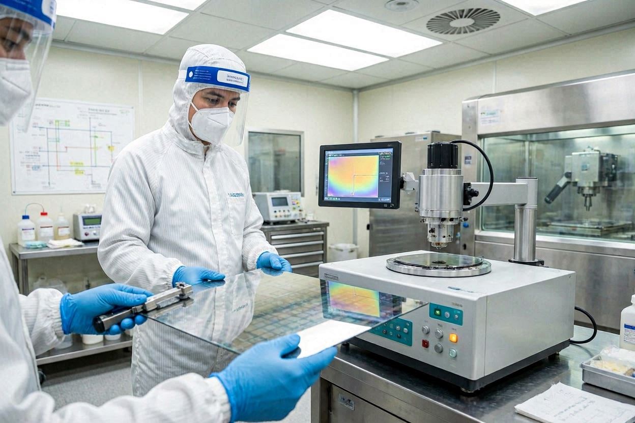
09SiC CMP Metrology and Quality
The quality requirements for epi-ready SiC substrates are among the most stringent in semiconductor manufacturing. The specifications ensure that the SiC surface is free of polishing-induced damage, chemical contamination, and morphological features that would propagate into the SiC epitaxial layer grown on top:
| Параметр | Specification (Epi-Ready 4H-SiC) | Measurement Method |
|---|---|---|
| Шероховатость поверхности Ra | <0.2 nm (Si-face) | AFM, 5×5 µm scan |
| Surface roughness Rq | <0.3 nm (Si-face) | AFM |
| TTV (Total Thickness Variation) | <5 µm (150 mm wafer) | Capacitance or optical mapping |
| BOW / WARP | <15 µm / <25 µm (150 mm) | Optical flatness metrology |
| Глубина подповерхностного повреждения | <5 нм | Cross-section TEM, X-ray diffraction rocking curve |
| Metal contamination (Fe, Ni, Cr) | <1×10¹⁰ атомов/см² | TXRF (total reflection XRF) |
| Particle density | <0.1 /cm² for particles >0.5 µm | Laser surface scanning (KLA Surfscan) |
10Market Context and Future Outlook
The SiC power device market has expanded dramatically through the early 2020s, driven by the electric vehicle (EV) traction inverter market — where SiC MOSFETs offer significant efficiency advantages over silicon IGBT-based designs at the 650–1700 V operating voltages typical of automotive powertrains. As of June 2026, the global SiC device market exceeds $3 billion annually and is growing at approximately 25–30% per year, with EV applications representing ~60% of demand. This growth is driving demand for: larger SiC wafer diameters (the industry transition from 150 mm to 200 mm SiC is ongoing); higher wafer throughput per polishing tool; and tighter epi-ready surface specifications to support next-generation 650 V, 1200 V, and 3300 V SiC device generations.
The transition from 150 mm to 200 mm SiC wafers creates new CMP challenges: the larger wafer diameter amplifies the uniformity demands on polishing tools, requiring carrier heads, pads, and slurry delivery systems designed for 200 mm operation. The SiC CMP consumable market — slurries, polishing pads, lapping films — is therefore one of the fastest-growing segments of the semiconductor CMP consumables industry in 2026.
SiC and WBG CMP Consumables from JEEZ
JEEZ specializes in CMP consumables for compound semiconductor and wide bandgap device manufacturing, including SiC substrate polishing applications. Contact us to discuss slurry formulation, pad selection, and process qualification for your SiC CMP module.
Contact JEEZ →