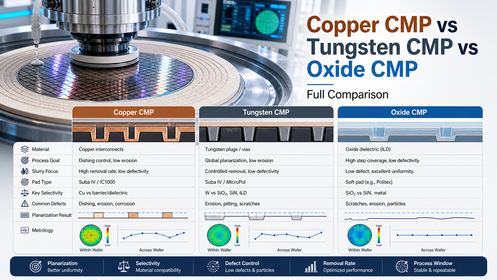
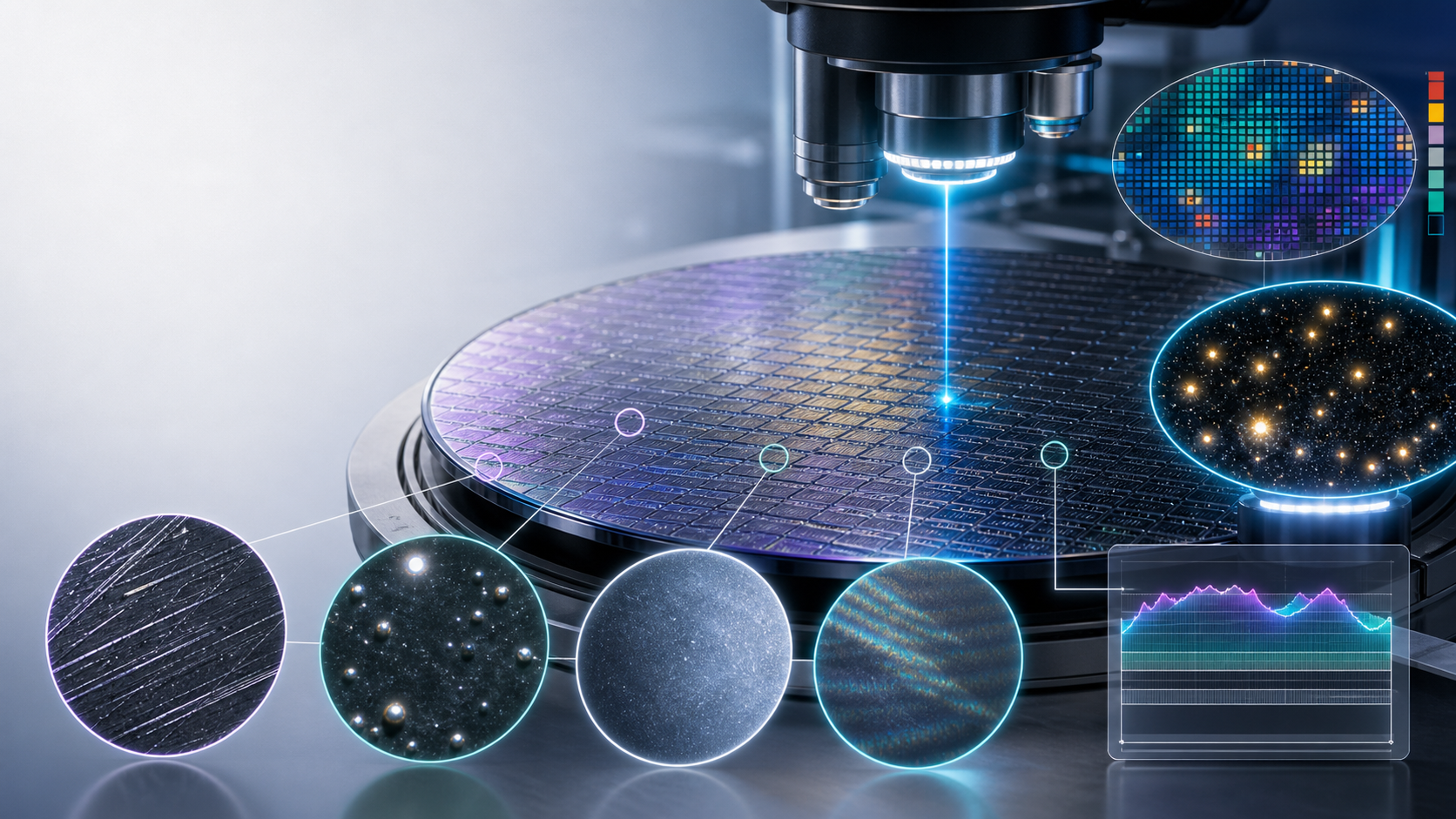
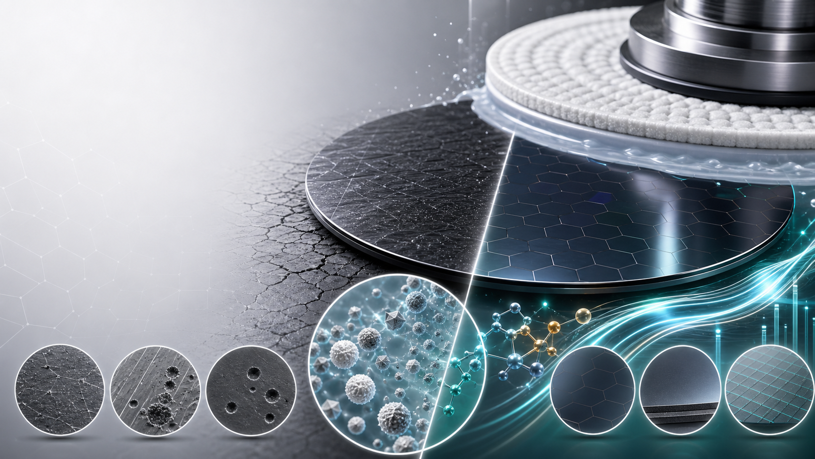
logo

О semiconductor

Этот автор еще не указал никаких подробностей.
На данный момент semiconductor создал 119 записей в блоге.

Role of Polishing Templates in CMP: How Fixture Design Impacts Wafer Flatness

CMP Process Engineering In chemical mechanical planarization, every nanometer of within-wafer non-uniformity has a device yield consequence. This guide explains exactly how polishing template geometry and backing pad design control ...

FR-4 против G-10 Шаблоны для полировки стекловолокна: Свойства материалов и руководство по выбору

Material Engineering Guide Two materials. Nearly identical names. Genuinely different performance envelopes. This guide explains exactly when each is the right choice — and when neither is sufficient. By Jizhi ...

Waxless Polishing Templates vs. Wax Mounting: Cost, Quality & Process Comparison

Process Technology Comparison Two fundamentally different approaches to holding a wafer during single-side polishing. One has been the industry standard for decades. The other has largely replaced it — and ...

How to Specify a Polishing Template: 6 Parameters Engineers Must Define

Engineering Specification Guide Incomplete or ambiguous polishing template specifications are the primary cause of first-article failures, TTV excursions, and unnecessary re-qualification cycles. This guide defines each parameter precisely — and ...

Standard vs. Custom Polishing Templates: Which Is Right for Your Wafer Process?

Procurement & Process Decision Guide A structured, engineering-led comparison of cost, lead time, TTV performance, and substrate fit — with a decision framework to guide your next procurement choice. By ...

Polishing Templates for Semiconductor & Silicon Wafer Processing: Complete Guide

Semiconductor Process Equipment Everything engineers, process owners, and procurement teams need to know — from material science and process mechanics to substrate-specific selection and custom engineering. By Jizhi Electronic Technology ...

Custom Polishing Templates for Silicon Wafers – Tailored to Your Carrier Head Specs

Custom Semiconductor Consumables When catalog templates fall short of your TTV, edge profile, or substrate requirements, custom engineering delivers the precision your process demands — from first drawing to production ...

Правила хранения, обработки и безопасности шлама CMP: Полное руководство по проектированию EHS

CMP slurry is not merely a precision chemical — it is a regulated hazardous material in most jurisdictions. H₂O₂-containing slurries are classified as oxidizers under GHS; acidic tungsten slurries are ...

Фильтры, хранение и обработка шлама CMP: Полное руководство по проектированию

A perfectly formulated CMP slurry can be rendered defective before it ever contacts a wafer — through improper storage temperatures that collapse colloidal stability, contaminated distribution materials that leach metal ...

Размер, рост и прогноз рынка шлама CMP на 2025-2032 гг: Полный отраслевой анализ

The global CMP slurry market is entering a sustained growth cycle driven by advanced logic scaling, 3D NAND capacity expansion, and an explosion in advanced packaging demand. This report delivers ...

Перейти к началу