CMP Defect Types,Root Causes & Yield Improvement
A systematic engineering reference for identifying, classifying, and eliminating CMP-induced defects — covering scratch defects, dishing, erosion, residues, delamination, and corrosion, with root-cause analysis frameworks, detection methods, and proven yield improvement strategies for production CMP modules.
How CMP Defects Impact Yield
CMP-induced defects are one of the leading sources of yield loss in advanced semiconductor manufacturing. Unlike many process defects that are localised and predictable, CMP defects can affect entire wafer regions or manifest as subtle topography changes that only become yield-critical several process steps later — making root-cause identification particularly challenging.
The economic impact is significant. At a leading-edge 300 mm fab producing 50,000 wafers per month, a 1% yield improvement at a single CMP step can be worth USD 5–15 million annually in additional revenue from good die. This high leverage makes CMP defect reduction one of the highest-ROI yield engineering activities in the fab. This guide complements the broader CMP context in our CMP Semiconductor Complete Guide.
CMP Defect Taxonomy
Micro-Scratches
Linear surface damage caused by large abrasive particles or agglomerates. Can sever metal lines, damage gate dielectrics, and cause reliability failures.
Delamination
Film separation at interface due to excessive polishing stress. Catastrophic for low-k dielectric films. Can cause entire die loss and tool contamination.
Блюда
Concave recess in wide metal or oxide features after CMP. Degrades electrical resistance of wide metal lines and transistor isolation in wide STI regions.
Erosion
Thinning of dielectric field in high-density array regions. Creates topographic variation that propagates to subsequent layers and affects lithography focus budget.
Residues & Particles
Slurry particles, chemical by-products, and metal ions remaining on the surface after post-CMP cleaning. Cause shorts, leakage, and reliability failures.
Copper Corrosion
Electrochemical dissolution of copper lines during or after CMP. Manifests as increased resistance, line thinning, or pitting. Can cause electromigration failures.
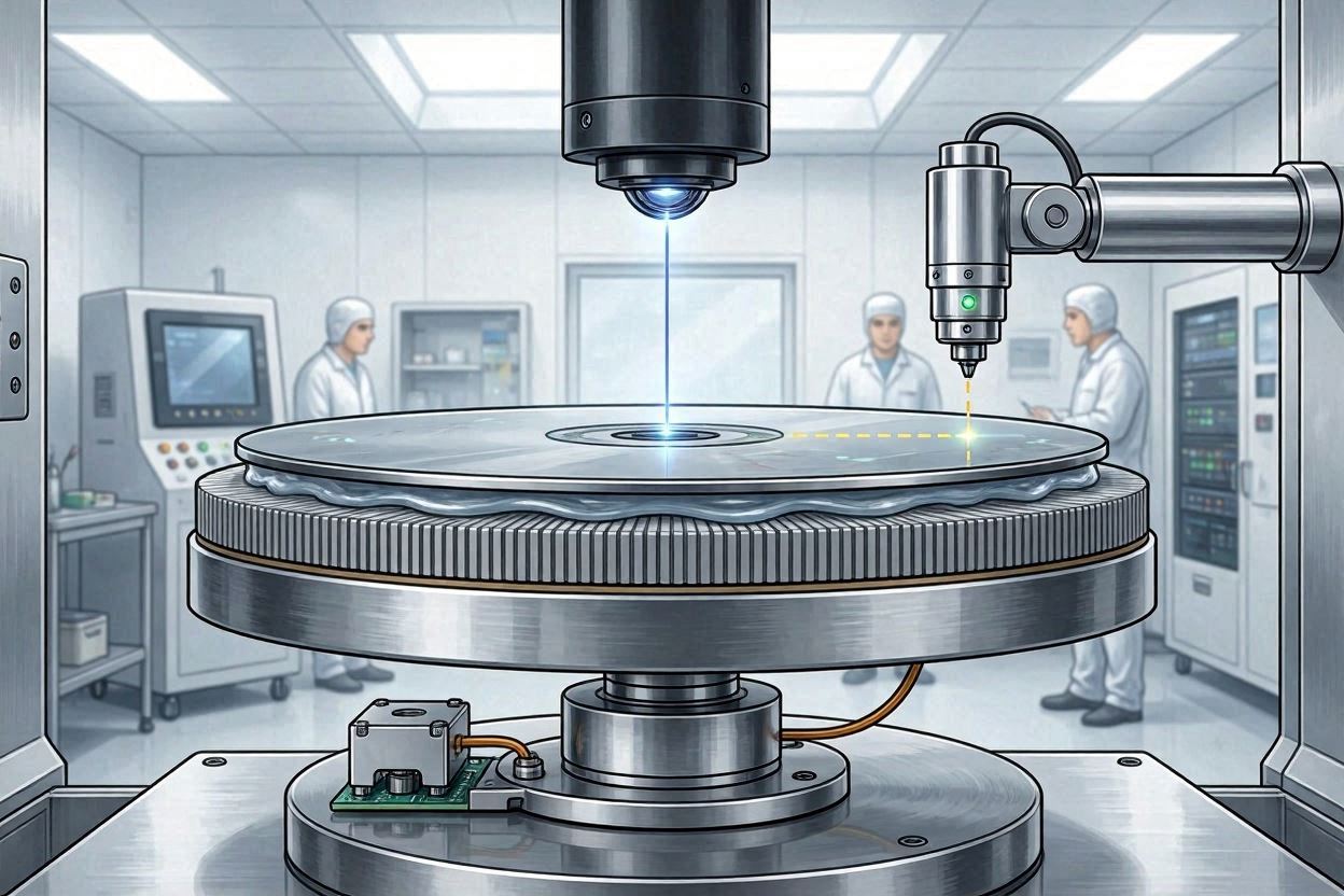
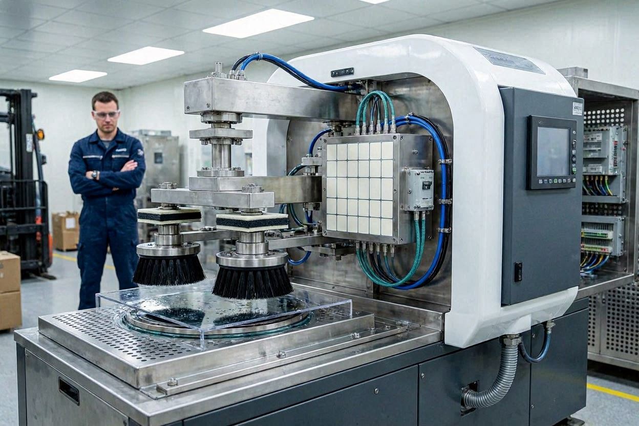
Scratch Defects: The Primary CMP Yield Killer
Micro-scratch defects are the single most impactful CMP defect type in terms of yield loss frequency and severity. A micro-scratch is a linear groove or chain of pits on the polished wafer surface, caused by a large abrasive particle, a hard agglomerate, or a foreign particle that becomes trapped between the polishing pad and the wafer surface and is dragged across it under polishing load.
Scratch Mechanism: The Three-Body Wear Model
CMP scratch formation is best understood through the three-body wear model: the wafer (body 1), the polishing pad (body 2), and the abrasive particle (body 3). During normal CMP, abrasive particles roll between the pad and wafer, removing material through a rolling contact mechanism with relatively low surface damage. A scratch occurs when a large particle (typically >1 µm) becomes embedded in the pad surface and slides rather than rolls, acting as a micro-cutting tool that ploughs a groove across the wafer surface.
The critical particle size for scratch formation is application-dependent but generally corresponds to particles larger than the pad asperity height — typically 0.5–2 µm. This is why the large-particle count (LPC) specification — defined as the number of particles per mL above 0.5 µm or 1.0 µm, measured by single-particle optical sensing (SPOS) — is the single most important slurry quality parameter for scratch defect control.
Root Causes of Scratch Excursions
- Slurry agglomeration: Freeze-thaw cycling, temperature excursions, contamination, or ageing can cause irreversible particle agglomeration, spiking the LPC by 10–100×. Always the first thing to check in a scratch excursion.
- POU filter failure or bypass: A clogged, damaged, or accidentally bypassed point-of-use filter allows large particles to reach the wafer. Check filter differential pressure and replace on schedule.
- Pad surface contamination: Hard particles embedded in pad surface from prior process contamination act as fixed abrasives. Inspect pad surface and condition aggressively to clear contaminated surface layer.
- Retaining ring debris: Worn retaining ring material (PEEK fragments) entering the polishing interface. Inspect retaining ring wear profile and replace when worn beyond spec.
- Dried slurry re-introduction: Dried slurry crust from the pad edge or delivery arm falling back onto the active pad surface. Review slurry dispensing arm position and pad rinse procedures.
Dishing & Erosion: Topography Defects
Dishing and erosion are topography defects — they do not appear as particles or surface damage in bright-field inspection but create height variations across the wafer surface that affect electrical performance and propagate to downstream lithography steps. Both phenomena are inherent to the CMP process and cannot be eliminated entirely; they must be controlled within a specification that the downstream process can tolerate.
Dishing: Mechanism and Control
Блюда is a concave surface profile at the centre of a wide metal or dielectric feature after CMP, caused by the polishing pad conforming into the recessed feature as the surrounding field material is cleared. The magnitude of dishing scales with feature width: a 1 µm copper line may dish by 2–3 nm, while a 100 µm dummy copper fill region may dish by 30–50 nm under the same polishing conditions. Wide copper bus lines and large metal fill regions in the BEOL stack are the most dishing-sensitive structures.
Dishing control strategies:
- Increase pad hardness — harder pads span wider features rather than conforming into them
- Optimise corrosion inhibitor (BTA) concentration — adequate BTA protects recessed copper from chemical dissolution
- Reduce over-polish time — dishing increases linearly with over-polish beyond the endpoint
- Apply design-for-CMP (DFCMP) rules — maximum metal feature width limits enforced in layout to keep dishing within spec
Erosion: Mechanism and Control
Erosion describes the excessive thinning of the inter-metal dielectric in regions of high metal pattern density. In dense arrays of copper lines (e.g., memory array bit-line regions), the locally high metal fraction means the polishing pad pressure is distributed over a smaller dielectric area between the metal lines, causing higher local removal rate in the dielectric. The result is that the dielectric in dense regions is thinner after CMP than in sparse regions, creating a systematic height variation that grows with each metal layer and eventually exceeds the lithography focus budget.
Erosion is controlled primarily through DFCMP density rules — enforcing maximum metal pattern density limits and requiring dummy metal fill in sparse areas to homogenise local pattern density and minimise erosion gradients. Slurry formulation changes that improve planarization efficiency (the rate at which raised features polish faster than recessed features) also reduce erosion.
Residues & Post-CMP Contamination
Post-CMP surface residues include all non-native materials present on the wafer surface after polishing and cleaning. They represent a direct threat to the next process step — deposition adhesion failure, gate dielectric integrity loss, or metal interconnect contamination — and must be reduced below the contamination budget for the next step before the wafer is released from the CMP module.
Particle Residues
Slurry abrasive particles (silica, ceria, alumina) that remain on the surface after post-CMP cleaning are the most common residue type. Their adhesion force depends on particle size (smaller particles adhere more tenaciously per unit mass), surface charge compatibility between particle and wafer surface (zeta potential mismatch promotes adhesion), and drying effects (particles dried onto the surface form much stronger adhesion bonds than wet particles). The particle removal efficiency (PRE) of the post-CMP cleaning process is the primary control metric. For the full treatment of cleaning chemistry and methods, see Post-CMP Cleaning: Methods, Challenges & Best Practices.
Metallic Residues
Dissolved metal ions — particularly copper, iron (from W CMP oxidisers), and cerium (from STI slurries) — adsorb onto silicon and oxide surfaces during CMP and must be removed by dedicated acidic cleaning steps. Copper surface contamination above 1×10¹⁰ atoms/cm² on silicon surfaces is sufficient to degrade transistor performance at advanced nodes. Measurement by total-reflection X-ray fluorescence (TXRF) is the standard method for monitoring metallic surface contamination at these trace levels.
Delamination
Film delamination during CMP — the sudden separation of a film from its substrate at an interface — is the most catastrophic CMP defect mode. A delamination event can expose the bare substrate across an entire device region, contaminate the CMP tool with debris that affects subsequent wafers, and in severe cases require a full tool clean and re-qualification before production can resume.
Delamination is primarily a risk for ultra-low-k (ULK) porous dielectric films (k < 2.2) and for thick metallic films with low adhesion energy at the barrier metal interface. The shear stress applied during polishing must be maintained below the critical adhesion energy (Gc) of the weakest interface in the film stack. At advanced nodes where ULK dielectrics are in the BEOL stack, CMP must use low downforce (<2 psi), soft pads, and slurries with reduced abrasive loading and surfactant additives that lower the coefficient of friction at the polishing interface.
For the specific challenges of low-k dielectric CMP at advanced nodes, see our article: CMP in Advanced Nodes: Challenges at 7nm, 5nm & Beyond.
Copper Corrosion Defects
Copper is an electrochemically active metal that undergoes dissolution in acidic environments — including the pH 2–5 conditions of many copper CMP slurries. When the balance between oxidation rate, mechanical removal, and corrosion inhibition is disrupted, copper corrosion defects appear as pitting, line thinning, surface roughening, or in severe cases complete line dissolution in recessed features.
The corrosion rate of copper in a CMP slurry environment is governed by the mixed potential between the anodic copper oxidation reaction and the cathodic reduction of the oxidiser (H₂O₂). At the mixed potential, the net dissolution rate depends on the kinetics of both reactions and is modulated by the surface coverage of the BTA corrosion inhibitor. Understanding and controlling this electrochemical balance is the core challenge of copper CMP slurry formulation. See the detailed discussion in Copper CMP vs Tungsten CMP vs Oxide CMP: Full Comparison.
Defect Detection Methods
| Defect Type | Detection Tool | Detection Principle | Sensitivity Limit |
|---|---|---|---|
| Micro-scratches, particles | KLA-Tencor Surfscan (bright-field) | Laser scattering — particles and surface defects scatter light off-axis | >30 nm particles; >50 nm scratches |
| Micro-scratches (buried) | Dark-field inspection (e-beam) | E-beam scattering sensitive to sub-surface damage | >10 nm buried defects |
| Dishing / erosion | AFM (atomic force microscopy) | Contact or tapping-mode surface height measurement | Sub-0.1 nm height resolution |
| Film thickness / WIWNU | Ellipsometry (KLA F5x, Nova T600) | Optical polarisation change on reflection | ~0.1 nm thickness; ~5 mm spatial resolution |
| Metal film thickness | 4-point probe / eddy current | Sheet resistance → film thickness (for metals) | ~0.1 Å/sq sheet resistance sensitivity |
| Metallic surface contamination | TXRF (total reflection XRF) | X-ray fluorescence from surface-adsorbed metal atoms | ~10⁹ atoms/cm² for Cu, Fe, Ni |
| Delamination | Acoustic emission; bright-field wafer inspection | Acoustic signal during CMP; large-area optical scan post-CMP | Macroscopic delamination detected in real-time |
Root Cause Analysis Framework
When a CMP defect excursion is detected, a structured root cause analysis (RCA) is essential to identify the correct corrective action. The following framework guides the investigation from symptom to root cause to fix.
Yield Improvement Strategies
Systematic CMP yield improvement requires a simultaneous focus on defect prevention (through process optimisation and consumable quality), defect detection (through inspection and metrology density), and defect disposition (through the right process response to out-of-spec lots).
Proven yield improvement levers
1. Tighten slurry incoming inspection: Implement 100% LPC measurement on incoming slurry lots. Reject lots above LPC spec before they reach the tool. Cost of rejection is a fraction of the yield loss from a scratch excursion.
2. Implement SPC on removal rate and WIWNU: Western Electric rules applied to CMP tool SPC charts catch pad glazing and process drift before they cause yield-impacting events. Mean shift of >1.5σ should trigger immediate engineering review.
3. Dual-source qualification for critical slurries: Single-source dependency creates supply-chain-induced process excursion risk. Qualifying a second slurry supplier with equivalent performance is the most robust supply risk mitigation.
4. Optimise post-CMP clean PRE: Measure particle removal efficiency (PRE) monthly on monitor wafers. PRE degradation below 95% indicates brush wear, chemistry drift, or DI water quality issue requiring immediate corrective action.
5. DFCMP guideline enforcement: Work with design teams to enforce metal density, feature width, and dummy fill rules that keep dishing and erosion within process capability limits. A 5% adjustment to layout density rules can eliminate systematic erosion hotspots entirely.
Struggling with CMP Defects or Yield Loss?
JEEZ supplies low-LPC CMP slurries and qualified polishing pads engineered for defect-sensitive production environments. Our application team supports yield improvement programs worldwide.
Contact JEEZ →