Semiconductor Planarization for Advanced Nodes: FinFET, GAA & 3D IC Challenges
Each generation of transistor scaling places fundamentally more stringent requirements on every CMP step in the process flow. The transition from planar to FinFET to Gate-All-Around nanosheet transistors, combined with the rise of 3D IC integration and extreme scaling of interconnect pitches, has transformed CMP from a smoothing step into a precision manufacturing operation where nanometer-level control is non-negotiable. This guide covers the CMP challenges at each advanced node as of June 2026.
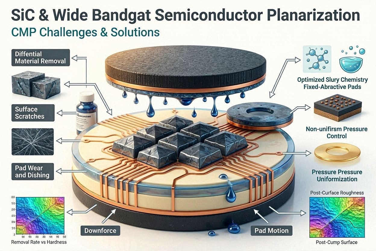
01The Scaling Challenge for CMP
For every transistor generation, the requirements placed on CMP become simultaneously more numerous and more demanding. The number of CMP steps increases as process complexity grows; the uniformity specifications tighten as the feature dimensions being controlled by CMP shrink; and new CMP modules appear for novel process elements — replacement metal gate, nanosheet release, self-aligned contacts, hybrid bonding — that did not exist in previous generations.
This step count increase represents not just more tool time and consumable cost, but a multiplicative yield challenge: each additional CMP step introduces a yield loss opportunity. At 25+ steps, even a 0.2% yield loss per CMP step compounds to a ~5% cumulative yield loss from CMP alone — making defect density reduction at each individual step a critical priority.
Simultaneously, the WIWNU specifications tighten with each generation. At 0.25 µm, ILD CMP WIWNU of 5% was acceptable. At 5 nm FinFET, STI CMP WIWNU must be below 1.5% to maintain acceptable fin height uniformity. At 2 nm GAA, nanosheet thickness uniformity from the nanosheet release CMP must be below 0.5 nm absolute — a requirement that pushes hard against the fundamental capabilities of CMP tool hardware and slurry formulation.
02FinFET Planarization: 22 nm to 5 nm
The transition from planar CMOS to FinFET transistor architecture, introduced by Intel at 22 nm in 2011 and subsequently adopted by all major logic foundries through the 5 nm node, introduced two fundamentally new CMP requirements that had no equivalent in planar process flows.
STI CMP for Fin Height Definition
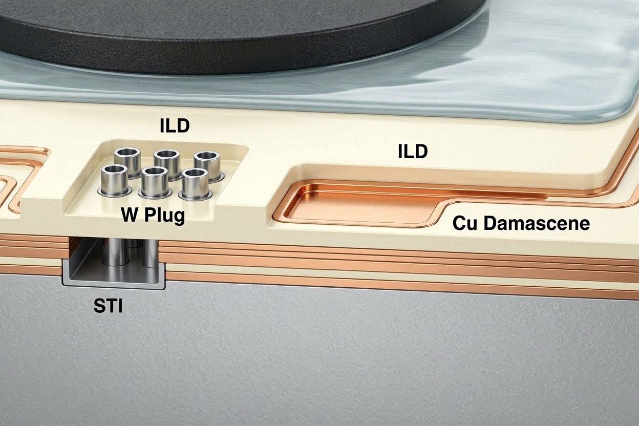
In FinFET technology, the silicon fin — a narrow, tall, vertical channel structure — is formed by etching the silicon substrate and STI trenches simultaneously. After HDP-CVD oxide fill and STI CMP, the STI oxide is recessed (etched back) to expose the fin sidewalls. The final fin height above the recessed STI is the difference between the Si surface and the recessed STI oxide level. Because the Si surface and STI oxide level are both defined by the STI CMP step (the post-CMP Si surface = the STI nitride mask top = the reference level), the entire fin height budget is set by the uniformity of a single CMP step.
Fin height variation directly translates to transistor Ion variation: a ±1 nm fin height variation across the 300 mm wafer translates to approximately ±2–4 mA/µm Ion variation — significant compared to the typical Ion specification windows of ±5–10 mA/µm. This makes STI CMP WIWNU the single most important planarization metric for FinFET yield and performance uniformity. The transition from colloidal silica to high-selectivity ceria slurry was driven largely by this FinFET fin height requirement.
Replacement Metal Gate (RMG) CMP
The FinFET gate-last (RMG) process, required to place thermally sensitive high-k dielectrics and metal gate materials after source/drain annealing, added two CMP steps not present in previous generation processes. The first RMG CMP planarizes the ILD to expose the dummy polysilicon gate tops — a step where WIWNU in the ILD thickness must be below ±1 nm to ensure consistent gate exposure across the wafer. The second RMG CMP planarizes the deposited metal gate (typically TiN + tungsten or cobalt fill) to the ILD surface level, setting the final gate height with a WIWNU specification tied directly to threshold voltage distribution.
The FinFET architecture effectively converts what was a surface planarity specification (ILD WIWNU) into a transistor performance specification (VT uniformity, Ion distribution). At 5 nm and below, the CMP process engineer and the device yield engineer are solving the same problem from different angles.
Self-Aligned Contact (SAC) CMP
Advanced FinFET flows use Self-Aligned Contact (SAC) processes to form source/drain contacts that are self-aligned to the gate spacers, reducing the design rule requirements for contact-to-gate spacing. SAC CMP removes the SAC cap dielectric to expose the contact metal plugs, requiring tight uniformity control to avoid over-polishing the gate dielectric cap (which provides isolation between the contact and the gate) while fully clearing the contact overburden.
03GAA Nanosheet CMP: 3 nm to 2 nm
Gate-All-Around (GAA) nanosheet transistors — in high-volume manufacturing at leading foundries at 3 nm equivalent nodes and under development for 2 nm and beyond as of June 2026 — require a fundamentally new CMP process with no precedent in FinFET technology: the selective removal of SiGe sacrificial layers from a vertically stacked Si/SiGe nanosheet stack to release the silicon nanosheet channels.
Nanosheet Release CMP Chemistry
The nanosheet stack consists of alternating Si and Si₁₋ₓGeₓ (typically x = 0.25–0.35) layers, each 5–8 nm thick, deposited by epitaxy. To form the GAA transistor channel, the SiGe layers must be selectively removed (etched), leaving only the Si nanosheets suspended across the gate region. Before and after this selective etch, CMP is used to: (1) planarize the nanosheet stack during FEOL processing; (2) define the nanosheet stack height with sufficient WIWNU to ensure consistent nanosheet count and thickness across the wafer; and (3) planarize the gate metal fill deposited around the released nanosheet channels.
The CMP for nanosheet stack planarization requires slurry selectivity between Si and SiGe of 5:1 to 20:1 — so that the CMP step preferentially polishes SiGe over Si, controlling the nanosheet thickness with sub-nanometer precision. This selectivity requirement is fundamentally different from anything required in FinFET or planar CMOS CMP, and has driven the development of entirely new slurry formulations based on oxidizer-type and chelant-type chemistry targeting the different surface properties of SiGe vs. Si.
Uniformity Requirements at 2 nm
The nanosheet channel thickness — typically 5–7 nm — is directly set by the epitaxy layer thickness and any subsequent polishing or etch processes. A WIWNU of ±0.5 nm absolute in nanosheet channel thickness translates to approximately ±7–10% variation in channel thickness, which impacts transistor drive current, threshold voltage, and short-channel effects. Achieving ±0.5 nm absolute WIWNU requires multi-zone carrier head control with individual zone pressure resolution of <0.1 psi, slurry temperature stability of ±0.2°C, and real-time run-to-run feedback from post-CMP ellipsometric or spectroscopic reflectometry thickness mapping at 121+ measurement points per wafer.
New Gate Metal CMP at GAA Nodes
GAA transistors use ruthenium (Ru) or cobalt (Co) as the fill metal for the gate, replacing tungsten which was standard in FinFET RMG. Both Ru and Co have different CMP chemistries from W: they require different oxidizer types (Ru is resistant to H₂O₂ alone, requiring stronger oxidizers such as periodate or Fenton chemistry; Co is susceptible to corrosion in acidic conditions without strong corrosion inhibitor packages), and they exhibit different selectivity ratios against the surrounding ILD. New CMP slurry formulations for Ru and Co gate CMP are an active area of development in the advanced node CMP consumables industry as of June 2026.
04BEOL Interconnect Scaling Challenges
As metal pitches scale below 20 nm (metal half-pitch at 2 nm node: approximately 12–16 nm), copper CMP faces fundamental new challenges driven by the geometry of the metal lines themselves:
Increased Dishing Sensitivity
At sub-20 nm metal pitches, the individual copper lines are so narrow that even 1–2 nm of dishing produces a proportionally enormous change in the effective copper cross-section — increasing line resistance by 5–15% per line. At these scales, the distinction between “acceptable” and “unacceptable” dishing collapses to a single nanometer of process control.
Barrier Metal Scaling
As metal lines shrink, the TaN/Ta barrier metal (which does not conduct electricity) takes up an increasingly large fraction of the total wire cross-section. At 20 nm copper pitch, a 2 nm TaN barrier on each side of a 16 nm copper line occupies ~25% of the line width. The trend toward thinner barriers (ALD TaN: 1 nm) and new barrier materials (Ru liner, MnₓOy self-formed barrier) places new requirements on barrier CMP chemistry — removing these ultra-thin, novel-material barriers without over-polishing the copper or the surrounding dielectric.
New BEOL Metals: Ruthenium and Cobalt
Below 20 nm line width, copper’s resistivity increases sharply due to surface scattering effects — the electron mean free path (~40 nm for bulk Cu) exceeds the wire dimensions, causing bulk resistivity to be replaced by surface-scattering-dominated resistivity. Ruthenium and cobalt, which have shorter mean free paths, are being introduced as the fill metal for the lower metal levels (M0, M1, M2) at 2 nm and below nodes. Both metals require entirely new CMP chemistries that are still maturing in development as of June 2026.
053D NAND Flash Planarization
3D NAND flash memory stacks 96 to 300+ alternating oxide/nitride layers above the silicon substrate to form the storage layer pairs. The fabrication of these tall, thin multilayer stacks requires periodic planarization to control the cumulative topography buildup that would otherwise exceed the depth-of-focus budget for the channel hole and staircase lithography steps.
CMP Challenges Unique to 3D NAND
- Thick film polish: Each CMP step must remove several hundred nanometers of dielectric (the accumulated overburden from multiple oxide/nitride layer deposition cycles), requiring high-MRR slurry formulations optimized for extended polishing without pad glazing.
- Pattern density extremes: The array areas (high pattern density from the multilayer stack pillars) and staircase areas (sparse, step-defined features) are adjacent on the same die, creating extreme local pattern density contrast that CMP must planarize without excessive dishing in the array or residue in the staircase regions.
- Cumulative stress management: The thick, stiff oxide/nitride multilayer film stack introduces substantial wafer bow (up to 500 µm) that requires compensation in the CMP carrier head pressure profile to avoid systematic center-to-edge removal rate non-uniformity.
06Advanced Packaging: TSV and Hybrid Bonding
The vertical integration of multiple dies in 3D IC packages — driven by the need to stack logic, HBM memory, and power management ICs in a single package for AI accelerators, mobile SoCs, and high-performance computing — has created two demanding new CMP applications at the packaging level.
TSV Reveal CMP
As described in our applications guide, TSV reveal CMP thins the wafer back-side to expose copper via tips. At advanced nodes, TSVs are being scaled to smaller diameters (2–5 µm vs. legacy 5–10 µm) and higher densities, making the post-reveal surface planarity more sensitive to CMP-induced copper dishing and silicon over-polish.
Hybrid Bonding: The Ultimate Surface Challenge
In die-to-die and wafer-to-wafer hybrid bonding (used in AMD 3D V-Cache, Foveros, and SoIC as of June 2026), the CMP surface preparation requirements — Ra <0.3 nm, copper step <2 nm, defects <0.01/cm² — represent the absolute limits of what CMP technology can deliver today. These specifications are not merely design targets; they are physical requirements dictated by the thermodynamics of the bonding mechanism itself. Meeting them requires not just optimized CMP recipes but also post-CMP plasma activation and DIW cleaning sequences, and in-line metrology at every step to verify compliance before bonding.
07New Materials at Advanced Nodes
Ruthenium (Ru) — Gate and Interconnect
Used as gate fill metal (GAA) and potential BEOL interconnect at sub-20 nm pitches. Ru CMP requires strong oxidizers (periodate, Fenton chemistry) beyond H₂O₂ alone. Slurry pH and oxidizer concentration are highly sensitive process parameters. Active area of consumable R&D.
Cobalt (Co) — Contact and Lower Metal
Used as contact fill (replacing W at some nodes) and lower BEOL interconnect metal. Co is susceptible to galvanic corrosion when co-polished with Cu. Requires dedicated BTA-like corrosion inhibitor packages. Co CMP slurry development is actively ongoing.
EUV Underlayer Materials
EUV lithography uses spin-coated metal oxide hard mask underlayers (Sn, Zr, Hf oxide) and amorphous carbon hard masks that sometimes require CMP for planarization before the next EUV exposure step. CMP of these novel, non-standard materials requires new slurry chemistries with minimal contamination impact on EUV optics.
Air-Gap Dielectric
Air-gap BEOL architectures replace low-k dielectric between metal lines with air (k = 1.0), offering the ultimate capacitance reduction. CMP of the metal above air gaps must apply zero lateral mechanical force to avoid collapsing the air cavity structures — the most mechanically demanding of all advanced node CMP challenges.
08The Uniformity Roadmap
| Technology Node | CMP Steps / Chip | STI CMP WIWNU Target | ILD CMP WIWNU Target | Cu Dishing Spec |
|---|---|---|---|---|
| 0.25 µm planar | 3-5 | 5–8% | 5–8% | 30–50 nm |
| 90 nm FinFET precursor | 6–9 | 3–5% | 3–5% | 15–30 nm |
| 22 nm FinFET | 12–15 | 1.5–2.5% | 1.5–2% | 8–15 nm |
| 7 nm FinFET | 17–21 | 1–1.5% | 1–1.5% | 4–8 nm |
| 3 nm GAA | 22–26 | 0.7–1% | 0.7–1% | 2–5 nm |
| 2 nm GAA (June 2026) | 25+ | <0.7% | <0.7% | <3 нм |
Advanced Node CMP Consumables from JEEZ
JEEZ engineers CMP slurries and polishing pads for the uniformity, selectivity, and defect performance demands of leading-edge process nodes. Contact us to discuss advanced node CMP consumable qualification.
Contact JEEZ Technical Team →