CMP Pad Defect Control: Scratches, Uniformity, and Surface Quality
CMP Pad Defect Control: Scratches, Uniformity, and Surface Quality
A systematic guide to identifying, diagnosing, and eliminating the post-CMP defect types most commonly caused by polishing pad properties — from micro-scratches and particle residues to edge-exclusion non-uniformity and pitting.
Focus
- The CMP Defect Landscape
- Scratch Types and Their Pad Origins
- Particle Residues and Contamination
- Within-Wafer Uniformity: Sources and Metrics
- Edge Exclusion Non-Uniformity
- Pitting and Corrosion Defects
- Defect Diagnosis: Root Cause Matrix
- Pad Selection for Defect Minimization
- Post-CMP Inspection Strategy
- FAQ
Post-CMP surface defects are one of the top yield loss mechanisms in advanced semiconductor manufacturing. A single scratch propagating through a critical metal interconnect layer can open-circuit the conductor; a cluster of particles left on the wafer surface before a thermal anneal can cause localized dielectric breakdown. At leading-edge process nodes (7 nm and below), the allowed post-CMP defect density is measured in single digits per wafer — defect levels that were considered impossible targets just a decade ago.
The polishing pad is not the only source of CMP defects — slurry chemistry, conditioner disk condition, post-CMP cleaning, and tool mechanical issues all contribute. But pad properties are among the most controllable and impactful variables available to process engineers. This guide provides a systematic framework for understanding which pad properties contribute to each defect type and how to minimize them. For how pad properties affect removal rate alongside defects, see: CMP Material Removal Rate and Pad Parameters.
1. The CMP Defect Landscape
CMP-generated defects fall into four severity tiers based on their impact on device yield and reliability. Understanding where pad properties contribute — and where they do not — is the first step in targeted defect reduction.
2. Scratch Types and Their Pad Origins
Not all scratches have the same origin or require the same corrective action. The first step in scratch defect reduction is correctly classifying the scratch type from post-CMP inspection data.
| Scratch Type | Inspection Signature | Primary Pad-Related Cause | 纠正行动 |
|---|---|---|---|
| Deep linear scratch | Long, straight or curved groove; consistent width; depth >50 nm by AFM | Large debris particle (pad chunk, agglomerated slurry) trapped between pad and wafer | Increase in-situ DI water flush; improve slurry filtration; check conditioner disk for chipping |
| Micro-scratch field | Dense population of fine, short scratches distributed across full wafer; depth <20 nm | Over-conditioned pad (high Ra); hard pad at excessive pressure; abrasive particle size too large | Reduce conditioner down-force; lower down-force pressure; switch to finer abrasive or softer pad |
| Arc scratches | Scratches follow circular arc pattern corresponding to platen or carrier rotation | Periodic hard particle source rotating with pad — conditioner disk edge chipping or pad debris embedded in groove | Inspect and replace conditioner disk; clean groove network; check pad surface for embedded particles |
| Edge scratch ring | Scratch density elevated in a ring near wafer edge (1–5 mm from edge) | Retaining ring debris or retaining ring-pad contact creating abrasive debris at wafer perimeter | Check retaining ring wear; adjust retaining ring pressure; ensure pad is properly seated and flat at edge |
| Center pit cluster | Localized pitting at wafer center; associated with low-pH slurry | Slurry starvation at wafer center (groove design insufficient for center delivery) combined with chemical attack on unpolished film regions | Switch to finer-pitch groove pad; increase slurry flow rate; verify groove is not clogged at center |
3. Particle Residues and Pad-Related Contamination
Particle residues on the post-CMP wafer surface fall into three categories based on origin, with different pad design implications for each:
Slurry Abrasive Residues
Spent or agglomerated abrasive particles (silica, ceria) that were not swept away by groove transport. Linked to insufficient groove drainage. Fine-pitch grooves and spiral patterns reduce this defect type by improving byproduct evacuation frequency. Primarily controlled by groove design and slurry flow rate, not pad hardness.
Pad Polymer Debris
Fragments of polyurethane shed from the pad surface during conditioning or polishing. Higher in early pad life (break-in debris) and in over-conditioned pads. Poreless pads dramatically reduce this defect type by eliminating the pore-derived debris source. Pad polymer debris is the primary differentiator between porous and poreless pad defect performance.
Reaction Byproduct Deposits
Precipitates from dissolved film material (Cu²⁺-BTA complexes in Cu CMP, WO₄²⁻ in W CMP) that re-deposit on the wafer surface when groove drainage is insufficient. Controlled by groove depth and pitch — deeper, finer-pitch grooves provide more frequent and complete byproduct evacuation. Also controlled by slurry pH and complexing agent concentration.
4. Within-Wafer Uniformity: Sources, Metrics, and Pad Controls
Within-wafer non-uniformity (WIWNU) is measured as the standard deviation (1σ) of post-CMP film thickness across a multi-point wafer map, expressed as a percentage of mean remaining thickness. At advanced nodes, WIWNU targets of below 1% (1σ) are standard for CMP steps preceding critical lithography levels. Three pad-related mechanisms generate WIWNU:
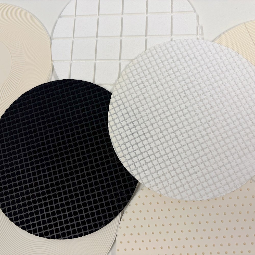
- Asperity height non-uniformity: If asperity height distribution is not uniform across the pad radius, contact pressure varies radially, causing radial MRR variation. This is controlled by pad surface Ra uniformity — a key QC metric that Jizhi measures across all production pads.
- Slurry delivery non-uniformity: Groove design that delivers slurry unevenly across the wafer diameter generates center-high or edge-high removal profiles. Addressed by groove pitch optimization or zone-varying patterns.
- Macro-scale pad flatness: A pad that is not flat (due to mounting defects or uneven wear) delivers non-uniform pressure distribution across the wafer, generating wafer-scale MRR gradients. Pad thickness uniformity (<0.05 mm 5-point variation) is a Jizhi production release criterion.
5. Edge Exclusion Non-Uniformity
Edge exclusion (EE) non-uniformity — systematically higher or lower removal at the wafer edge compared to the center — is one of the most persistent CMP uniformity challenges on 300 mm wafers. It has two primary origins that require different pad-related corrective actions:
| Edge Profile Type | Likely Cause | Pad-Related Correction |
|---|---|---|
| Edge-fast (over-removal at edge) | Retaining ring pressure higher than carrier down-force; hard pad with low compressibility; high wafer bow concentrating stress at edge | Switch to softer subpad or stacked pad to increase edge compliance; verify retaining ring pressure calibration; reduce conditioner down-force to lower edge-zone Ra |
| Edge-slow (under-removal at edge) | Slurry starvation near wafer edge — centrifugal force drains groove channels before reaching wafer periphery; low carrier-to-platen velocity ratio at outer wafer radius | Switch to spiral groove pattern to enhance centrifugal delivery to pad edge; increase slurry flow rate; reduce groove pitch in outer pad zone |
| Oscillating profile (ring pattern) | Groove interference pattern — standing wave in slurry delivery as specific groove-wafer alignment repeats at fixed intervals | Change groove pitch to a value incommensurate with carrier oscillation frequency; switch from concentric to XY or spiral pattern to eliminate angular interference |
6. Pitting and Corrosion Defects
Pitting — small, localized depressions in the polished film surface — is chemically rather than mechanically driven, but pad groove design plays a contributing role. Pitting occurs when slurry chemistry attacks the wafer film at a locally elevated rate in areas of low or stagnant slurry renewal. The relevant pad design connection: pads with insufficient groove drainage (shallow grooves, wide pitch) create zones of slurry stagnation under the wafer where spent, enriched slurry accumulates. In Cu CMP, this enriched slurry can cause local galvanic corrosion; in oxide CMP, it can cause etch-back of the dielectric at pH-excursion zones. Optimized groove design that ensures complete slurry renewal on every platen revolution is the pad-level mitigation.
7. Defect Diagnosis: Root Cause Matrix
| Observation | Most Likely Pad-Related Root Cause | Verification Test | Primary Corrective Action |
|---|---|---|---|
| Sudden scratch density increase (all types) | Conditioner disk damage / particle shedding | SEM inspection of conditioner disk surface | Replace conditioner disk; clean pad surface with DI flush |
| Gradual micro-scratch density increase over pad life | Over-conditioning or pad surface Ra drifting high | Profilometer Ra measurement of pad surface | Reduce conditioner down-force; verify conditioning frequency |
| Center-low MRR (concave profile) | Slurry starvation at wafer center — groove design or flow rate | Test with 50% higher slurry flow rate — if profile improves, groove/flow is limiting | Switch to finer-pitch or spiral groove pad; increase slurry flow |
| High particle count, distributed uniformly | Pad polymer debris from over-conditioned or worn pad | EDX analysis of particles — polymer vs. slurry | Replace pad; reduce conditioning intensity; consider poreless pad |
| High particle count at wafer center only | Byproduct re-deposition from groove stagnation at center | Increase slurry flow — if particles decrease, groove drainage is limiting | Finer-pitch groove pad; increase groove depth; increase slurry flow |
| Edge-fast removal profile worsening with pad age | Pad non-uniformity increasing as edge wears faster than center | 5-point pad thickness map — confirm edge-thin | Replace pad; adjust conditioning sweep profile to equalize wear |
8. Pad Selection for Defect Minimization
The following pad selection guidance prioritizes defect performance — recommended when post-CMP defect density is the primary process constraint, even at some cost to throughput:
- For scratch defect reduction: Select the softest pad hardness consistent with meeting planarization efficiency requirements. For Cu BEOL buff steps, Shore D 28–38 with fine-grit conditioner (D40–D60). For oxide steps where both planarity and low scratches are required, consider a stacked configuration (IC1000-type top + very soft subpad) to get hard-pad planarization with reduced edge contact stress.
- For particle residue reduction: Consider poreless pads, which eliminate the primary source of pad polymer debris. Switch to finer-pitch grooves to improve slurry byproduct evacuation. Verify post-CMP cleaning compatibility with your particle types.
- For WIWNU reduction: Select a pad with higher compressibility (softer subpad in stacked configuration, or softer top pad) to improve macro-scale wafer conformance. Switch to finer-pitch or spiral groove pattern for better slurry uniformity. For the full selection framework, see: Hard vs. Soft CMP Polishing Pads: Selection Guide.
9. Post-CMP Inspection Strategy
Effective defect management requires a structured post-CMP inspection program. The following inspection layers work together to catch different defect types:
- Optical surface inspection (KLA, Hitachi, AMAT): Dark-field and bright-field wafer scanning after every CMP step for production wafers. Captures scratches >20 nm depth and particles >50 nm diameter. The primary in-line defect detection tool.
- AFM (atomic force microscopy): Periodic off-line measurement of surface roughness Ra and sub-10 nm surface features. Required for qualifying new pads and verifying that conditioning protocol changes do not degrade surface quality.
- SEM-EDX: Used for particle origin analysis when optical inspection identifies elevated particle counts — distinguishes pad polymer debris from slurry abrasive from process film fragments by elemental analysis.
- Sheet resistance mapping (4-point probe): For metal CMP steps — measures electrical thickness uniformity as a proxy for WIWNU. Catches uniformity issues that optical inspection misses.