CMP Equipment Market Trends 2026
目录
Market Size and Growth Outlook
The global market for chemical mechanical planarization equipment has been on a steady upward trajectory, driven by continued semiconductor fab expansion, the transition to more advanced process nodes, and growing demand for advanced packaging capacity. Industry estimates place the CMP equipment market at roughly $7.96 billion in 2025, with projections pointing toward approximately $13.84 billion by 2033 — a compound annual growth rate (CAGR) of around 7.2% over that period.
This growth rate reflects more than simple unit volume increases. As device geometries shrink and chip designs incorporate more layers, each wafer typically requires more CMP steps than it did in previous generations, which means equipment demand grows faster than wafer starts alone would suggest.
Regional Demand Patterns
CMP equipment demand is heavily concentrated in regions with the largest concentrations of wafer fabrication capacity. Asia-Pacific remains by far the largest market, reflecting the region’s dominant share of global semiconductor manufacturing, followed by North America and Europe.
| Region | Approximate Market Share | Primary Demand Drivers |
|---|---|---|
| Asia-Pacific | ~52% | Large concentration of foundry, memory, and advanced packaging capacity; ongoing fab expansions and domestic equipment programs |
| North America | ~29% | Leading-edge logic fabs, advanced packaging investment tied to AI and HPC demand, and growing onshore capacity expansion |
| Europe | ~18% | Specialty and power semiconductor manufacturing, automotive-grade chip production, and targeted capacity expansion programs |
While Asia-Pacific’s share reflects its scale, the relative growth rates in North America and Europe are notable, as both regions have seen renewed investment in domestic semiconductor manufacturing capacity over recent years — a trend that has direct implications for CMP equipment and consumables sourcing strategies.
Wafer Size and Equipment Segment Trends
By wafer size, 300mm CMP systems account for more than 60% of the equipment market, consistent with 300mm being the standard platform for leading-edge logic and memory fabrication. This dominance is expected to continue as fab expansions overwhelmingly favor 300mm capacity for new builds.
That said, 200mm CMP equipment remains an active segment, particularly for power semiconductor, analog, MEMS, and compound semiconductor manufacturing — applications where 300mm conversion is not always economically justified. We cover the practical differences between these platforms in 300mm vs 200mm CMP Equipment Differences.
Competitive Landscape and Domestic Substitution
The CMP equipment supplier landscape continues to be shaped by a small number of established global players, including Applied Materials, EBARA, Lapmaster, LOGITECH, and Revasum, each of which holds significant installed base across different process segments and wafer sizes.
At the same time, one of the most consequential trends in the CMP equipment market over the past several years has been the rise of domestic equipment suppliers in China. Hwatsing Technology, a domestic CMP equipment manufacturer, recently shipped its 1,000th CMP system — a milestone that reflects both the maturity of domestic equipment programs and the broader push toward semiconductor equipment self-sufficiency in the region. Other domestic players, including AMEC and Anji Microelectronics, have also expanded their presence across CMP equipment and related consumables.
For buyers, this competitive shift has practical implications: a wider range of qualified equipment options is becoming available, particularly for fabs in regions where domestic sourcing is a strategic priority, and consumables suppliers increasingly need to support process compatibility across both established international platforms and newer domestic equipment.
AI, HPC, and Advanced Packaging Demand
Perhaps the most significant demand driver shaping the CMP equipment market in 2026 is the surge in AI and high-performance computing (HPC) chip production, and the advanced packaging techniques that go with it. Technologies such as CoWoS (chip-on-wafer-on-substrate), high-bandwidth memory (HBM) stacking, hybrid bonding, and through-silicon via (TSV) reveal processes all rely heavily on CMP steps that did not exist — or existed in much smaller volumes — in traditional front-end-only flows.
Industry estimates suggest that advanced packaging adoption is driving CMP steps-per-wafer up by roughly 35% in flows that incorporate these technologies, compared to traditional front-end-only process flows. Each additional CMP step represents incremental demand not just for equipment, but for the polishing pads, slurries, and conditioners consumed at each step.
We explore the equipment and process implications of this shift in more detail in CMP Equipment for Advanced Node Manufacturing.
SiC and GaN Power Electronics Growth
Beyond logic and memory, demand for CMP equipment is also being shaped by growth in silicon carbide (SiC) and gallium nitride (GaN) power semiconductor manufacturing, driven primarily by electric vehicle (EV) powertrains and broader power electronics applications. SiC and GaN substrates present distinct polishing challenges compared to silicon — they are significantly harder and more chemically resistant, which affects pad selection, slurry chemistry, and polishing parameters.
As EV production scales and power electronics content per vehicle increases, fabs producing SiC and GaN devices represent a growing — though still comparatively smaller — segment of overall CMP equipment demand, with specific consumable requirements that differ from mainstream silicon CMP.
What These Trends Mean for Buyers
Taken together, these trends point toward a market where overall demand is growing steadily, the competitive landscape is broadening, and the mix of applications driving that demand is becoming more diverse — spanning traditional logic and memory, advanced packaging, and power semiconductors.
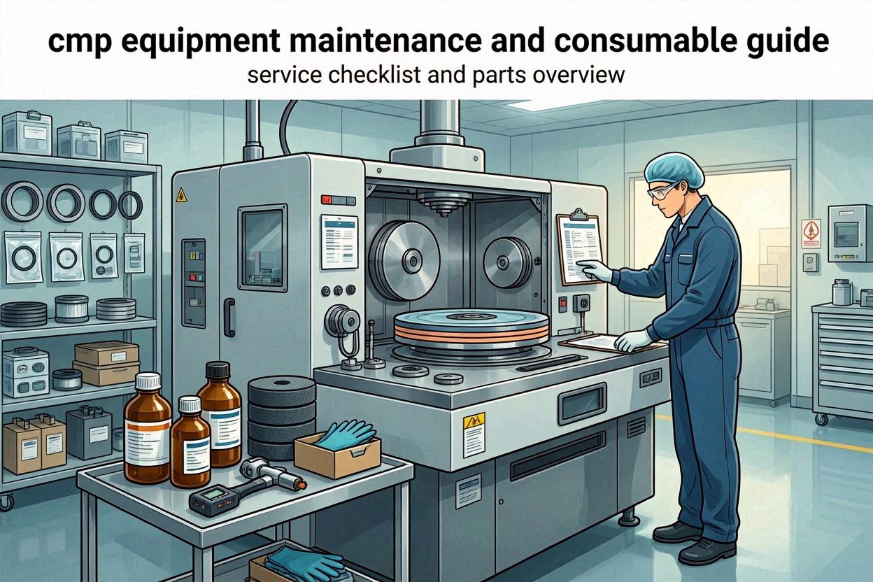
For procurement and process teams, this has several practical implications. First, equipment and consumable sourcing decisions increasingly need to account for a wider range of qualified suppliers. Second, as advanced packaging adds CMP steps to existing flows, consumable consumption per wafer is rising even where wafer volumes are flat — a factor worth building into budget planning, which we discuss further in CMP Equipment Maintenance and Consumables Guide. Third, evaluating suppliers on criteria beyond price — including consumable ecosystem support and technical responsiveness — becomes more important as the supplier landscape diversifies, a topic covered in How to Choose a CMP Equipment Supplier.
For a broader view of how CMP equipment fits into overall fab operations, return to our complete CMP equipment guide.
Planning Your CMP Consumables Strategy for 2026 and Beyond?
JEEZ supports fabs navigating shifting equipment and process requirements with a broad consumables portfolio and responsive technical support. Get in touch with our team.
联系我们常见问题
How big is the CMP equipment market expected to be by 2033?
Industry estimates project the CMP equipment market to grow from approximately $7.96 billion in 2025 to roughly $13.84 billion by 2033, representing a compound annual growth rate of around 7.2%.
Which region accounts for the largest share of CMP equipment demand?
Asia-Pacific accounts for approximately 52% of CMP equipment demand, reflecting its concentration of global semiconductor manufacturing capacity, followed by North America at around 29% and Europe at around 18%.
Why is advanced packaging increasing demand for CMP equipment?
Advanced packaging techniques such as CoWoS, HBM stacking, hybrid bonding, and TSV reveal rely on additional CMP steps not present in traditional front-end-only flows, with industry estimates suggesting these techniques can increase CMP steps-per-wafer by roughly 35%.
How is the competitive landscape for CMP equipment changing?
Alongside established global suppliers such as Applied Materials, EBARA, Lapmaster, LOGITECH, and Revasum, domestic equipment manufacturers in China — including Hwatsing, AMEC, and Anji Microelectronics — have expanded their presence, broadening the range of qualified equipment options available to fabs.