Role of Polishing Templates in CMP: How Fixture Design Impacts Wafer Flatness
In chemical mechanical planarization, every nanometer of within-wafer non-uniformity has a device yield consequence. This guide explains exactly how polishing template geometry and backing pad design control the flatness metrics that matter most at leading-edge nodes.
CMP Fundamentals: Why Flatness Is a Fixture Problem
Chemical mechanical planarization is one of the most specification-sensitive processes in semiconductor manufacturing. At the 7 nm node and below, the within-wafer non-uniformity (WIWNU) budget for oxide CMP is measured in angstroms — a 3σ range of 2–5 nm across a 300 mm wafer is the production target for leading-edge STI and ILD planarization. At these tolerances, every component in the polishing system that introduces mechanical non-uniformity must be understood and controlled.
The polishing template is one of three mechanical elements in CMP that directly control wafer flatness — the others being the polishing pad (typically a stacked polyurethane/subpad assembly) and the carrier head membrane pressure system. Unlike the pad and the carrier head, which are visible process variables routinely analyzed in CMP process development, the polishing template is often treated as a background component whose contribution to flatness is assumed to be negligible. This assumption is wrong, and it is a source of unexplained flatness excursions in CMP processes that have otherwise been carefully optimized.
To understand how polishing templates work at the fundamental level is to see immediately why fixture design is a flatness variable: the template is the mechanical interface between the carrier head and the wafer backside, and every geometric imperfection in that interface transmits directly to the wafer surface as a pressure non-uniformity.
Where the Polishing Template Sits in the CMP System
The CMP system is a stack of mechanical components, each contributing to the overall pressure field at the wafer-pad interface. Understanding the template’s position in this stack makes its influence on flatness mechanistically clear.
The polishing template occupies the carrier plate and backing pad layers in this stack. Its function is to receive the carrier head’s downforce at the top surface and deliver a controlled, uniform pressure field at the wafer backside. Any geometric imperfection in the template — bow in the carrier plate, non-uniform backing pad thickness, incorrect work-hole depth — modifies the pressure field before it reaches the wafer, creating systematic material removal non-uniformities that map directly onto the finished wafer’s flatness signature.
Three Mechanisms of Template Influence on Flatness
The polishing template influences CMP flatness through three distinct and separable physical mechanisms. Understanding each mechanism independently makes it possible to diagnose which template parameter is responsible for a given flatness signature in production data.
Pressure Redistribution via Backing Pad Compliance
The backing pad’s compliance determines how the carrier head’s applied pressure is distributed across the wafer backside. A pad that is too stiff transmits carrier head pressure non-uniformities directly to the wafer; one that is too soft allows the wafer to “float” and creates its own pressure non-uniformity. The correct pad compliance averages out carrier head non-uniformities while maintaining the pressure magnitude needed for target removal rate.
Primary driver of WIWNUWork-Hole Depth Setting Wafer Mechanical Position
Work-hole depth sets the wafer’s resting position relative to the polishing pad contact plane under load. A work hole that is too deep recesses the wafer below the optimal contact position, reducing applied pressure and material removal rate. Too shallow, and the wafer protrudes into higher-pressure contact, increasing removal rate at the expense of edge profile. Errors in this dimension create systematic, radially symmetric TTV patterns.
Primary driver of systematic TTVCarrier Plate Bow Introducing Long-Range Thickness Gradient
Carrier plate bow — deviation from perfect flatness across the plate working surface — introduces a gradual pressure gradient across the wafer diameter. A carrier plate with 15 µm of bowl-shaped bow creates higher pressure at the wafer center and lower pressure at the edge (or vice versa for a dome shape), producing a systematic thickness gradient that degrades both TTV and SFQR across the entire wafer area.
Primary driver of bow-related TTVPressure Distribution: The Core Mechanism
Preston’s equation — the foundational relationship in CMP modeling — states that the local material removal rate at any point on the wafer surface is proportional to the product of the local contact pressure and the local relative velocity between the wafer surface and the polishing pad: MRR = k × P × V, where k is the Preston coefficient (a combined measure of pad, slurry, and material properties). At any given polishing machine operating point, velocity is a function of position and rotation speed and is essentially fixed. This means that within-wafer removal rate variation is dominated by pressure variation — and pressure variation at the wafer surface is determined by the template’s pressure delivery to the wafer backside.
The backing pad is the primary pressure-redistribution element in this system. Its compliance determines how a non-uniform input pressure from the carrier head membrane is transformed into the output pressure field at the wafer backside. The key insight is that backing pad compliance acts as a spatial low-pass filter on the pressure field: a compliant pad averages out high-frequency (short spatial scale) pressure non-uniformities from the carrier head, while a stiff pad transmits them with high fidelity.
Backing pad compliance correctly matched to process pressure and carrier head characteristics. Center and edge pressures within ±3% of target. Result: uniform removal rate, TTV ≤ 1.0 µm.
Backing pad too stiff — transmitting carrier head retaining ring pressure spike to wafer edge. Center-high profile from over-compression at work-hole center. Result: TTV 2.5–4.0 µm, edge rolloff at 2 mm.
This filtering property has a critical implication for CMP template specification: the correct backing pad hardness is not a universal constant, but a function of the specific carrier head used and its characteristic pressure non-uniformity profile. A carrier head that has been recently refurbished and has a nearly uniform membrane pressure delivers a different input pressure distribution than an older carrier head with worn retaining ring and membrane variability. The same template that delivers excellent WIWNU on the refurbished head may show systematic non-uniformity patterns on the worn head, not because the template is wrong, but because the pad compliance is no longer matched to the changed input pressure profile.
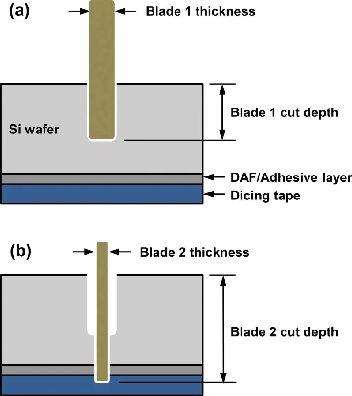
Work-Hole Depth Precision and TTV
The work-hole depth — measured from the backing pad working surface to the bottom of the pocket — is the template dimension most directly linked to global wafer TTV. Its influence is both large in magnitude and systematic in character: work-hole depth errors produce radially symmetric TTV patterns that affect every wafer polished on a given template and are reproducible from lot to lot until the template is replaced.
The Depth-TTV Transfer Function
Under polishing load, the wafer backside sits on the wetted backing pad and the wafer front face contacts the polishing pad. The work-hole depth sets the clearance between the bottom of the work-hole pocket and the wafer backside: if the work hole is exactly the right depth for the target final thickness under the applied load, the wafer surface is co-planar with the template face (or set to the desired offset), and pressure is distributed uniformly. Any deviation from this ideal depth shifts the wafer’s equilibrium position relative to the polishing pad contact plane.
The transfer function is approximately linear near the design point: a 5 µm work-hole depth error produces approximately 4–6 µm of systematic TTV across the wafer diameter, depending on backing pad compliance and applied pressure. At tight TTV specifications of ≤1.0 µm, this means that work-hole depth must be held to within ±1–2 µm of the nominal design value to ensure the template is not the dominant TTV contributor.
Carrier Plate Bow and Long-Range Flatness
Carrier plate bow is a low-spatial-frequency flatness error — it introduces a gradual thickness gradient across the full wafer diameter rather than the sharp local non-uniformities associated with backing pad defects or work-hole depth errors. Because it is a long-range effect, carrier plate bow affects flatness metrics at all scales: global TTV, site-level SFQR, and edge profile at the wafer perimeter.
Bow Direction and TTV Pattern
Carrier plate bow can be either concave (bowl-shaped, where the plate center is lower than the periphery) or convex (dome-shaped, where the center is higher). Each produces a characteristic TTV signature:
- Concave bow: Higher pressure at the wafer center relative to the edge. Under Preston’s law, this produces higher material removal at the wafer center, leaving the center thinner than the edge — a center-thinned, edge-thick TTV pattern sometimes called “doming” in the final polished wafer profile.
- Convex bow: Lower pressure at the wafer center, higher at the periphery. This produces center-thick, edge-thinned TTV — a “cupping” profile that is the opposite of the concave case.
In practice, carrier plate bow below 10 µm produces TTV contributions of 0.3–0.8 µm for standard silicon SSP, which is acceptable for most production specifications. At advanced CMP nodes with TTV targets of ≤0.5 µm, carrier plate bow must be specified at ≤5 µm and verified by CMM measurement on every production lot — not just the initial qualification sample.
Sources of Carrier Plate Bow
Carrier plate bow has three main sources. The first is residual stress in the raw laminate material from the curing process — this is controlled by selecting raw material with validated flatness specifications from quality-controlled laminate producers. The second is thermal distortion during machining — heat generated by CNC milling can induce local stress relaxation in the laminate that causes post-machining bow. Controlled-temperature machining with intermediate stress-relief steps minimizes this source. The third is service-induced bow from asymmetric chemical attack in the polishing environment — more relevant for templates operating near the edge of their chemical compatibility range, as described in our FR-4 vs G-10 material guide.
Backing Pad Selection for CMP Applications
Backing pad selection for CMP templates requires balancing three competing performance requirements that cannot all be maximized simultaneously: pressure redistribution uniformity, planarization efficiency, and wafer retention force. The correct selection point in this three-way trade-off depends on which CMP process type is being run and which flatness metric is the binding constraint.
Shore A Hardness and Its Effects
Shore A hardness is the primary backing pad specification variable for CMP applications. Its effects on each performance dimension are systematic and well-characterized:
| Shore A Range | Pressure Uniformity | Planarization Efficiency | Wafer Retention | Best CMP Application |
|---|---|---|---|---|
| 30–45 (Soft) | 优秀 | Poor | 中度 | Back-side CMP, flip polish, fragile substrates |
| 45–55 (Medium-Soft) | Very good | 中度 | 良好 | Metal CMP (Cu, W) — uniformity-dominant |
| 55–65 (Medium) | 良好 | 良好 | 良好 | Oxide CMP, STI CMP — optimal balance |
| 65–75 (Medium-Hard) | 中度 | Very good | 优秀 | High-selectivity STI, barrier CMP |
| 75–85 (Hard) | Poor | 优秀 | 优秀 | SiC CMP, high-pressure bulk removal |
Pad Thickness and Uniformity
Backing pad thickness interacts with Shore A hardness to determine the effective compliance of the pad assembly. For the same Shore A value, a thicker pad provides more compliance (more deflection per unit of applied pressure) than a thin pad, with the relationship approximately linear for small deflections. Pad thickness uniformity — specified as the maximum deviation from nominal thickness across the pad area, typically ±15 µm for production CMP templates — directly affects WIWNU by creating local regions of higher or lower compliance that produce corresponding local variations in removal rate.
Pad thickness non-uniformity creates a characteristic “fingerprint” pattern in CMP output: the same within-wafer non-uniformity pattern repeats across every wafer polished on a given template, with a spatial frequency and orientation correlated to the pad’s thickness non-uniformity map. This signature is often initially misdiagnosed as a carrier head or polishing pad issue until template isolation testing (running the same process recipe with a new replacement template) reveals that the pattern disappears when the template is changed.
Planarization Efficiency: How Templates Affect Step-Height Removal
In CMP, planarization efficiency is the ability to preferentially remove material from topographically high areas (raised features) while leaving low areas (recessed features) relatively untouched. This is quantitatively measured as the step-height reduction rate: how quickly the height difference between a raised pattern and a recessed field collapses toward zero as polishing progresses. High planarization efficiency is essential for shallow trench isolation (STI), inter-layer dielectric (ILD), and W-plug fill applications where complete step elimination is required within a defined overpolish budget.
The Template’s Role in Planarization Mechanics
Planarization efficiency in CMP is primarily governed by the stiffness of the polishing system above the wafer — how rigidly the polishing pad is supported at the scale of the feature being planarized. A stiffer support system produces higher contact pressure on raised features (which protrude above the mean surface level) and reduced or zero pressure on recessed features, maximizing the differential removal rate between high and low areas. A more compliant support system conforms to the surface topography, reducing the pressure differential between high and low areas and slowing planarization.
The polishing template’s backing pad contributes directly to the effective stiffness of the polishing system above the wafer. A stiffer backing pad (higher Shore A) increases the effective system stiffness at the spatial scales relevant for die-level planarization (feature sizes of 1–100 µm), improving planarization efficiency. This is why advanced STI CMP processes typically specify harder backing pads than metal CMP processes of comparable pressure — STI requires aggressive step elimination, while metal CMP prioritizes within-wafer thickness uniformity over planarization efficiency.
Template Contributions to SFQR at Leading-Edge Nodes
Site Flatness Front Reference least squares (SFQR) is the flatness metric most directly linked to lithography overlay and depth-of-focus budget at advanced technology nodes. SFQR is measured within individual exposure fields (typically 26 × 8 mm for 300 mm wafer scanners) and specifies the maximum peak-to-valley height variation within each field after subtracting the best-fit tilted plane through that field’s data. For 5 nm node and below, SFQR specifications of ≤25 nm across all measured sites are common production requirements.
At these flatness levels, template-related contributions to SFQR become measurable and, in some cases, dominant. Three template parameters each have a distinct SFQR signature:
Carrier Plate Bow → Wafer-Scale SFQR Gradient
A carrier plate with 10 µm of bow produces a gradual thickness gradient across the 300 mm wafer diameter. Over a 26 × 8 mm site, this gradient contributes a tilt component — not a random variation within the site, but a systematic height difference between the leading and trailing edges of the site in the bow direction. After the best-fit plane subtraction in the SFQR calculation, this manifests as a consistent SFQR offset at sites positioned along the bow axis, degrading the wafer-level SFQR distribution by 5–15 nm depending on bow magnitude and site orientation.
Backing Pad Thickness Non-Uniformity → Repeating Site-Level Pattern
As noted in Section 7, backing pad thickness variation creates a spatial fingerprint in removal rate that repeats across every wafer polished on the template. If the spatial wavelength of the pad thickness non-uniformity is comparable to the SFQR site size (26 × 8 mm or 26 × 26 mm), the pad’s non-uniformity maps directly into site-level SFQR degradation. Backing pad thickness uniformity of ±15 µm is the specification threshold below which pad-related SFQR contribution is typically below 5 nm. Above 20 µm non-uniformity, pad-related SFQR contribution can reach 15–30 nm — a significant fraction of the total SFQR budget at advanced nodes.
Work-Hole Depth Error → Radially Correlated SFQR Degradation
A work-hole depth error introduces a radially symmetric TTV pattern (as described in Section 5). Because the TTV profile is radially symmetric, its gradient within any given SFQR site is primarily a tilt component rather than a random variation. The SFQR calculation removes this tilt through the best-fit plane subtraction, meaning that work-hole depth errors contribute less to SFQR than they do to TTV. However, for work-hole depth errors above 10 µm, the second-order curvature of the radially symmetric TTV profile creates a residual within-site non-flatness that is not removed by the best-fit plane subtraction and contributes directly to SFQR — typically at the 3–8 nm level per 5 µm of depth error.
Template Requirements by CMP Process Type
CMP is not a single process but a family of processes with significantly different material systems, slurry chemistries, and flatness requirements. The polishing template specification must be matched to the specific CMP process type being run.
For metal CMP applications using H₂O₂-based acidic slurries (pH 2–5), it is critical to validate carrier plate material compatibility against the slurry chemistry before production deployment — standard FR-4 templates will degrade in these conditions on a 40–60 cycle timeline, as detailed in our FR-4 vs G-10 material selection guide.
SSP vs. CMP Template: Key Specification Differences
Single-side polishing (SSP) and CMP share the same basic template architecture — carrier plate plus backing pad — but the performance requirements that drive template design differ significantly between the two process types. Engineers transitioning from SSP to CMP template specification need to understand these differences to avoid applying SSP template assumptions to a CMP context where they do not hold.
| 参数 | SSP Template | CMP Template | Reason for Difference |
|---|---|---|---|
| Primary flatness metric | TTV (global) | SFQR + WIWNU + TTV | CMP directly affects lithography field-level flatness; SSP is a blank wafer process |
| Typical applied pressure | 2–5 psi | 1–7 psi (wider range) | CMP includes low-pressure barrier and high-pressure bulk oxide steps |
| Slurry chemistry range | Predominantly alkaline (pH 8–12) | pH 2–12 depending on layer | Metal CMP uses acidic slurries; oxide and barrier span the pH range |
| Backing pad hardness | Shore A 55–75 (moderate) | Shore A 45–75 (process-specific) | CMP planarization efficiency requires careful hardness matching per process type |
| Carrier plate bow spec | ≤10 µm (standard) | ≤5 µm (advanced nodes) | SFQR budget at 5 nm node demands tighter bow control than SSP TTV budget |
| Edge enhancement ring | Required for EE <2 mm | Required for EE <2 mm | Same requirement — both processes push edge exclusion |
| Chemical resistance priority | Moderate (mostly alkaline) | High — slurry chemistry varies by CMP step | Metal CMP H₂O₂ and acidic slurries demand G-10 or CXT; FR-4 insufficient |
| Template replacement frequency | Cycle-life limited | Often shorter — higher chemical and mechanical wear | CMP’s higher pressures and aggressive chemistries accelerate both dimensional and chemical degradation |
Isolating Template-Related Flatness Problems in Production
When a CMP process begins showing systematic flatness excursions — TTV drift, SFQR degradation, or repeating within-wafer patterns — the diagnostic challenge is distinguishing template-related causes from the many other potential sources: polishing pad conditioning state, carrier head membrane wear, slurry concentration drift, and platen temperature variation all produce flatness signatures that can superficially resemble template-related effects. A structured isolation protocol prevents wasted re-qualification effort on the wrong process variable.
Step 1: Identify the Spatial Character of the Excursion
Template-related flatness excursions have a characteristic spatial signature that distinguishes them from other sources. Carrier plate bow produces a smooth, radially symmetric or directional gradient across the full wafer diameter. Backing pad thickness non-uniformity produces a repeating pattern that correlates to the pad’s spatial structure and appears identically on every wafer polished on that template. Work-hole depth error produces a radially symmetric, center-to-edge TTV slope. If the observed excursion matches one of these spatial signatures, the template is the prime suspect.
Step 2: Check Template History
Correlate the onset of the flatness excursion with the template’s cycle count and any recent template changes. Template-related TTV drift typically increases gradually as the backing pad wears and work-hole depth increases — a sudden step change in TTV is more likely a carrier head or pad change than a template issue. Review the SPC chart of TTV vs. template lot to see if the excursion is lot-correlated. Maintaining detailed template lot tracking is covered in our guide to extending polishing template lifespan.
Step 3: Run a Template Swap Test
The definitive isolation test is replacing the suspect template with a known-good replacement while holding all other process parameters constant. If the flatness excursion disappears with the new template, the original template is confirmed as the root cause. If the excursion persists unchanged, the template is not responsible. This test requires only one additional wafer lot and is always faster and cheaper than simultaneously investigating multiple potential root causes. Our troubleshooting article, Why Is Your Wafer Edge Profile Poor?, extends this diagnostic framework specifically to edge-related flatness failures.