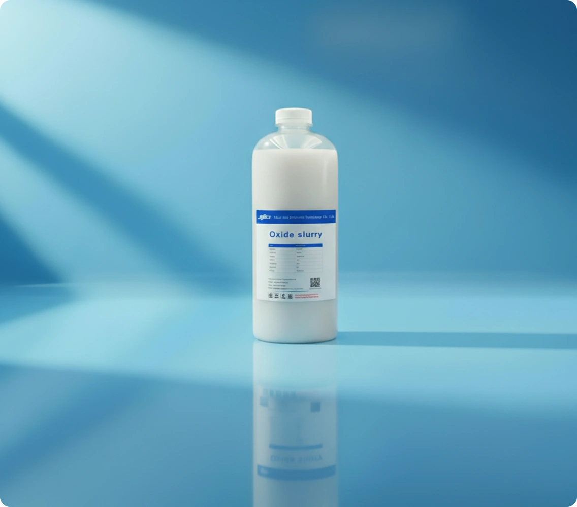


氧化物泥浆
Oxide Polishing Slurry / Oxide CMP Slurry
Semiconductor CMP Polishing Slurry
主要功能
- After polishing and cleaning, the wafer surface has low roughness and minimal particle residue.
- Suitable for polishing of 4-12 inch silicon oxide coated wafers.
产品名称
Oxide Polishing Slurry / Oxide CMP Slurry
Function of Oxide Polishing Slurry
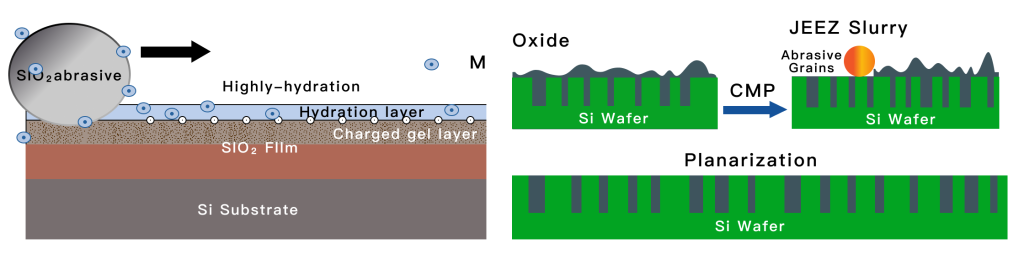
Widely used for CMP polishing of oxide materials to achieve precise surface planarization and thickness control,
such as silicon oxide layers on wafer surfaces or oxide layers between top metal layers and silicon oxide. It is suitable for oxide polishing of 4–12 inch silicon oxide coated wafers.
The Oxide Slurry uses carefully selected SiO₂ colloidal silica with uniform particle size as the abrasive, enabling polishing results with low surface roughness and minimal particle residue.
By optimizing the dilution ratio during use, customers can achieve optimal polishing performance. Compared with similar products domestically and internationally, this product features easy cleaning and low surface roughness.
产品特点
Nanometer-grade SiO2 abrasives with uniform and stable particle size, stable removal rate, and low metal ion content. Through the CMP process, it effectively removes the surface oxide layer, achieving ideal flatness.
Compared to similar products both domestically and internationally, JIZHI Electronics Oxide Slurry features easy cleaning and low surface roughness.
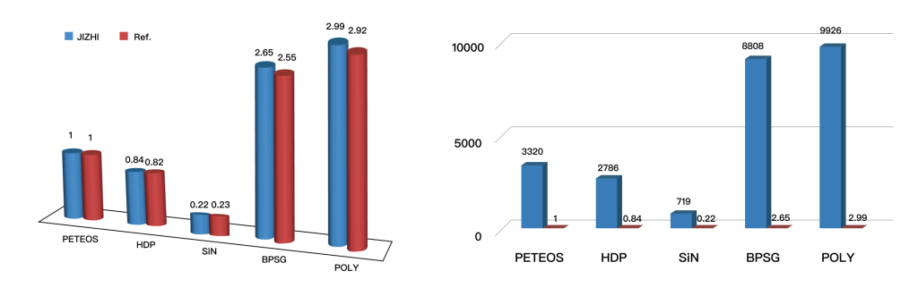
Selectivity Comparison
Features of Oxide Slurry Polishing Liquid:
1.High polishing rate
2.S and Oxide ratio selection of 1:1
3.Low metal particle content
(Total metal content is comparable to imported products)
| 项目 | Parameters |
|---|---|
| Machine | Hwatsing |
| Test Wafer | 6 hours |
| 材料 | Si-filled PSG |
| Ra (nm) | 0.26 |
| R.R (A/min) | 5523 |
| Range (A) | 6% |
| Dishing | -100 to 200 |
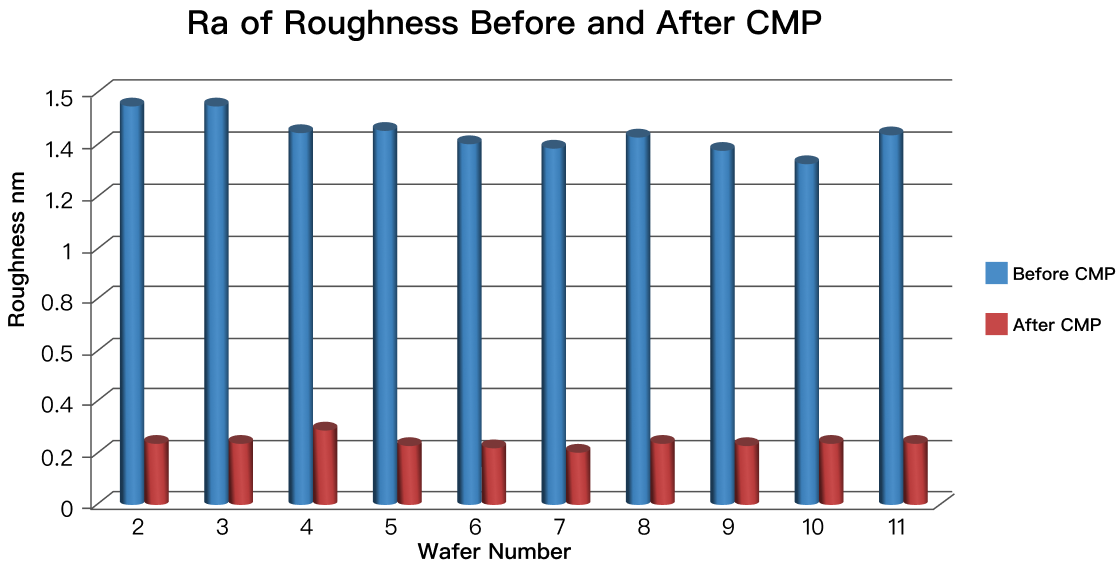
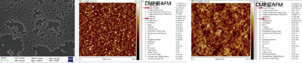
The surface roughness Ra after CMP is 0.3nm, which is within the standard range.
为什么选择集智电子?
10 年光学材料 CMP 经验
10 年光学材料 CMP 经验
抛光方案和配方可灵活定制
无毒、可生物降解配方,符合国际环保标准。
免费进程调试
40% 的处理时间比传统方法更快a
引进国外生产技术和设备
优化的消耗率降低了总体运行成本。