logo

About semiconductor

This author has not yet filled in any details.
So far semiconductor has created 195 blog entries.

Copper CMP Slurry: Dual Damascene Process, Formulation & Defect Control — Complete Engineering Guide

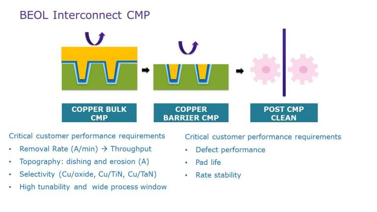
Copper CMP is the most chemically complex and process-sensitive step in BEOL semiconductor manufacturing. A three-stage polishing sequence — each requiring a fundamentally different slurry chemistry — must deliver bulk ...

By |2026-03-04T11:35:44+08:002026年3月4日|Blog, Industry|Comments Off on Copper CMP Slurry: Dual Damascene Process, Formulation & Defect Control — Complete Engineering Guide

CMP Slurry Composition: Abrasives, Chemical Additives & Formulation Principles

What actually goes into a CMP slurry — and why does every ingredient matter? This is the definitive technical guide to CMP slurry composition: abrasive particle science, chemical additive functions, ...

By |2026-03-04T11:39:33+08:002026年3月4日|Blog, Industry|Comments Off on CMP Slurry Composition: Abrasives, Chemical Additives & Formulation Principles

What Is CMP Slurry? A Complete Guide to Chemical Mechanical Planarization Slurry

From wafer-level planarization at the 3nm node to advanced packaging for chiplets, CMP slurry is the consumable that makes modern semiconductor manufacturing possible. This guide covers everything you need to ...

By |2026-03-04T10:32:56+08:002026年3月4日|Blog, Industry|Comments Off on What Is CMP Slurry? A Complete Guide to Chemical Mechanical Planarization Slurry

CMP Slurry Types Explained: Oxide, STI, Copper, Tungsten & Beyond

Not all CMP slurries are created equal. Each semiconductor polishing step demands a uniquely formulated slurry — different abrasive chemistry, different pH, different selectivity profile. This guide breaks down every ...

By |2026-03-04T11:43:57+08:002026年3月3日|Blog, Industry|Comments Off on CMP Slurry Types Explained: Oxide, STI, Copper, Tungsten & Beyond

Dicing Saw Blade Width in Semiconductor Dicing

Dicing saw blade width is a critical parameter that directly determines kerf control, cutting precision, and blade path stability during wafer dicing. Although blade width is often discussed together with ...

By |2026-01-28T10:29:07+08:002026年1月28日|Blog, Industry|Comments Off on Dicing Saw Blade Width in Semiconductor Dicing

Dicing Saw Blade Thickness for Wafer Cutting

Dicing saw blade thickness is one of the most critical yet frequently misunderstood parameters in wafer dicing. Blade thickness directly determines kerf loss, influences die mechanical strength, and must remain ...

By |2026-01-28T10:29:05+08:002026年1月28日|Blog, Industry|Comments Off on Dicing Saw Blade Thickness for Wafer Cutting

Wafer Dicing Blades for Dicing Equipment

In semiconductor wafer singulation, the performance of diamond dicing blades is inseparable from the characteristics of the dicing equipment. Even a well-designed blade will fail to deliver stable cutting results ...

By |2026-01-28T10:29:01+08:002026年1月28日|Blog, Industry|Comments Off on Wafer Dicing Blades for Dicing Equipment

Dicing Blade Specifications for Wafer Dicing Applications

Accurate specification of dicing blades is a critical factor in semiconductor wafer singulation. Beyond nominal thickness and width, the interplay between diamond grit, concentration, bond type, equipment limits, and wafer ...

By |2026-01-28T10:27:21+08:002026年1月28日|Blog, Industry|Comments Off on Dicing Blade Specifications for Wafer Dicing Applications

Diamond Dicing Blades for Semiconductor Wafers

Diamond dicing blades for wafers are not generic cutting tools; they are highly engineered consumables designed to meet the mechanical, thermal, and material-specific requirements of semiconductor wafer singulation. As wafer ...

By |2026-01-28T10:28:58+08:002026年1月28日|Blog, Industry|Comments Off on Diamond Dicing Blades for Semiconductor Wafers
Go to Top