
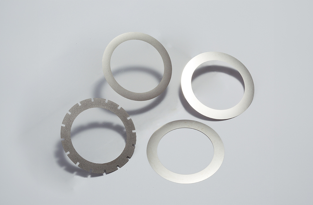
Diamond Dicing Blades for Wafer Dicing
Diamond dicing blades are the core cutting tools used in modern semiconductor wafer singulation. From a product engineering perspective, a diamond dicing blade is not a generic consumable but a ...
Diamond dicing blades are the core cutting tools used in modern semiconductor wafer singulation. From a product engineering perspective, a diamond dicing blade is not a generic consumable but a ...
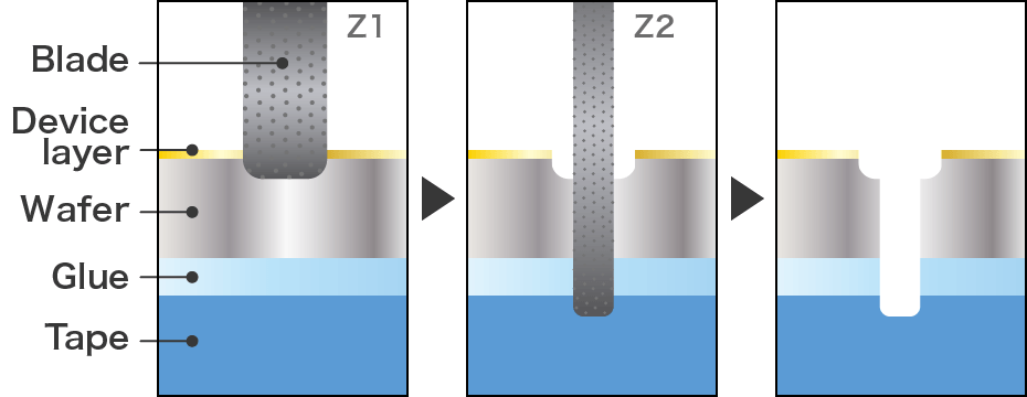
The blade dicing process is the most widely adopted wafer singulation method in semiconductor manufacturing. Despite the emergence of alternative technologies such as laser dicing and stealth dicing, blade dicing ...
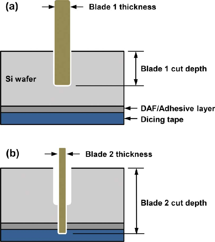
Dicing blade technology forms the technical foundation of wafer singulation in semiconductor manufacturing. While the dicing process itself appears mechanically simple, the cutting behavior at the blade–wafer interface is governed ...
Wafer dicing blades are precision cutting tools used in semiconductor manufacturing to separate processed wafers into individual dies. Although dicing is one of the final steps in wafer fabrication, its ...
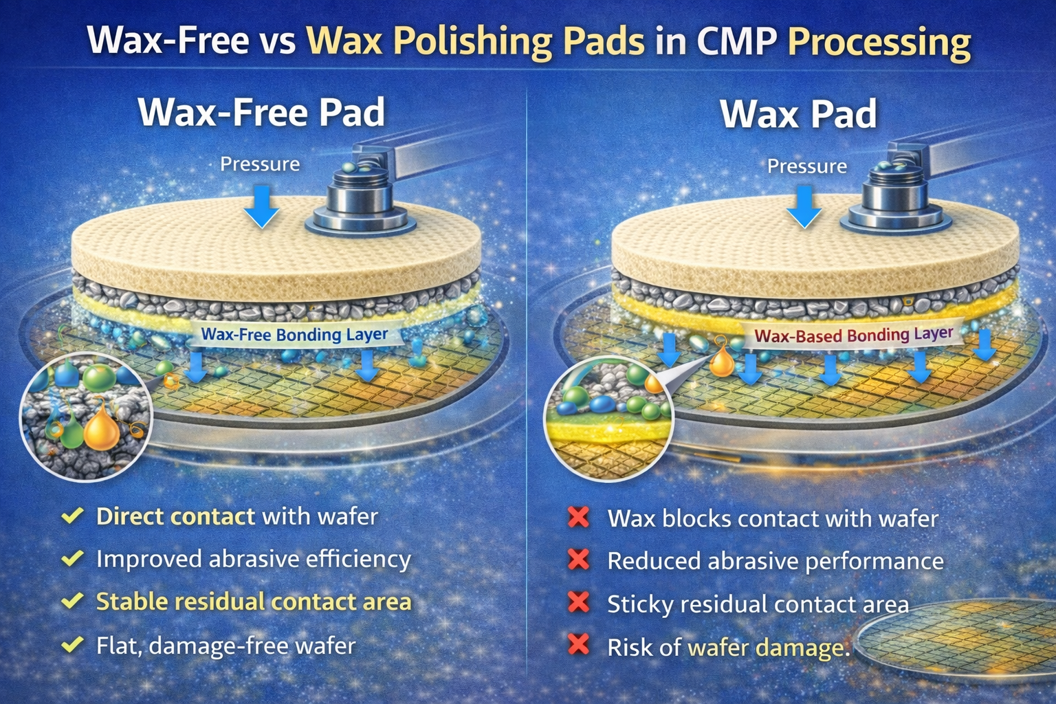
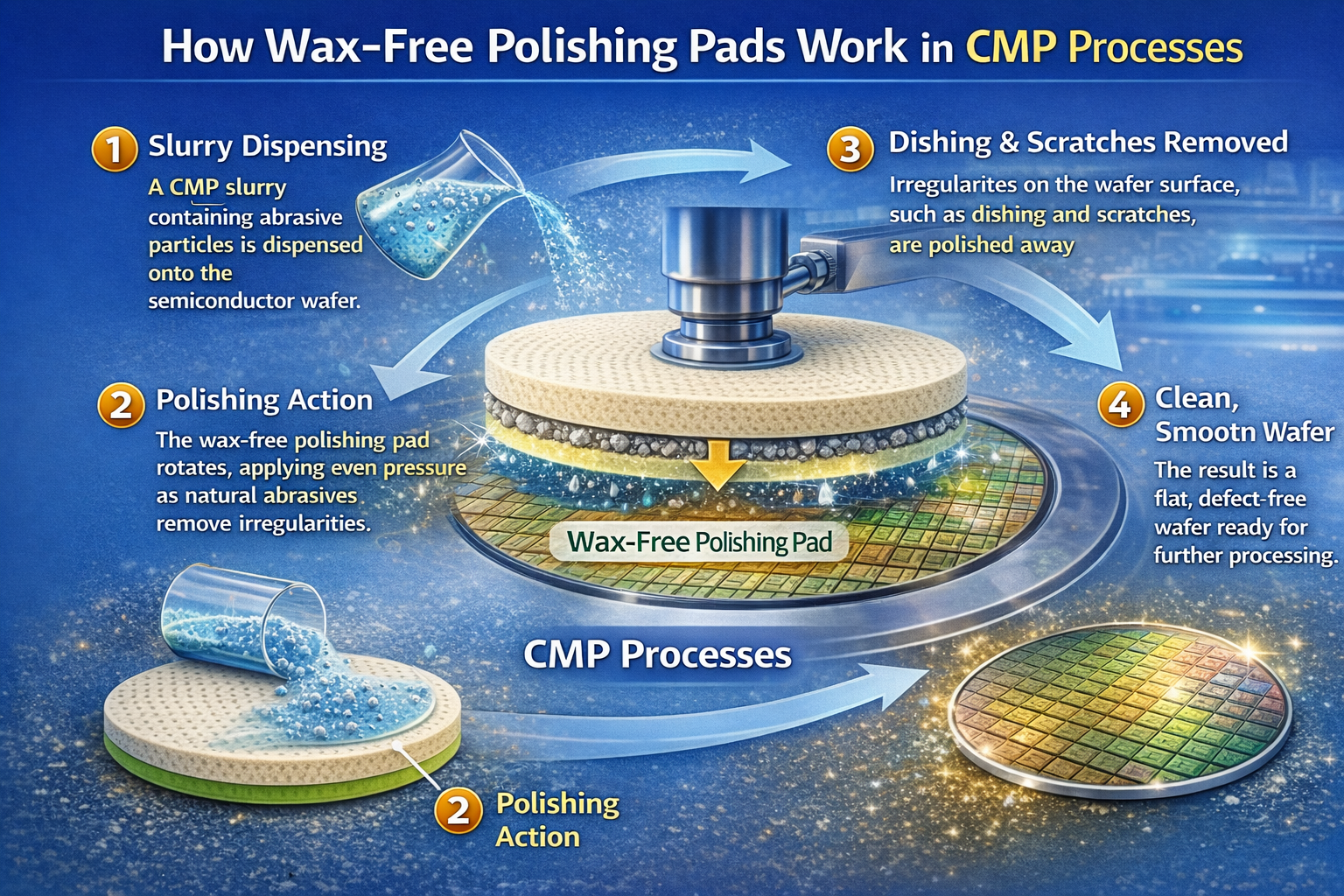
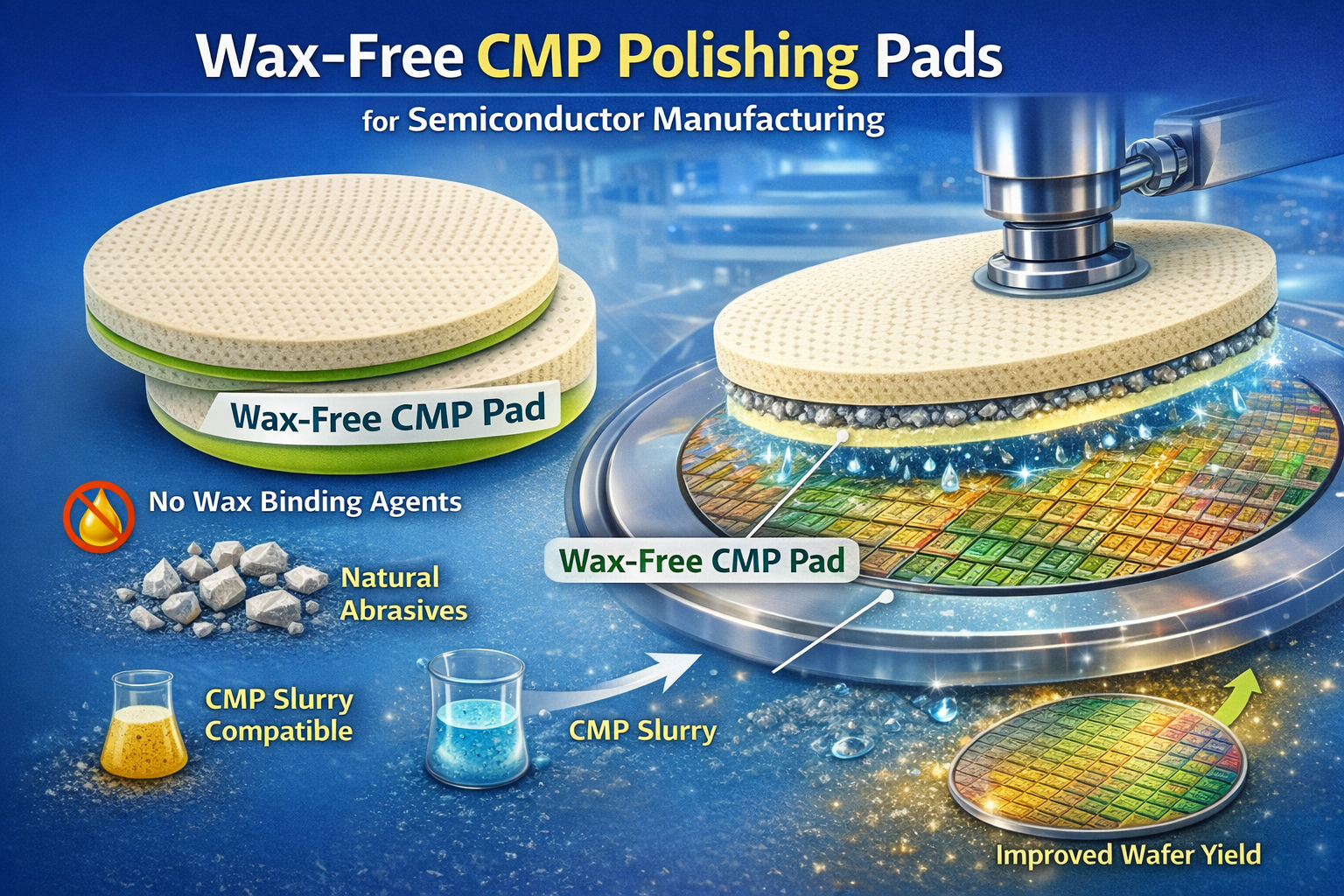
In CMP, polishing pad materials define the fundamental mechanical, chemical, and tribological interactions that ultimately determine planarization efficiency, defectivity, and process stability. For wax-free CMP polishing pads, material selection becomes ...
In modern semiconductor manufacturing, CMP is no longer an isolated unit operation but a tightly integrated process module interacting with upstream deposition, downstream cleaning, and overall yield management. The adoption ...
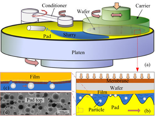
In chemical mechanical planarization (CMP), the polishing pad is not merely a consumable surface but a critical process component that directly affects wafer flatness, material removal rate (MRR), defectivity, yield ...
Table of Contents 1. Introduction: Why Wax-Free Pad Working Principles Matter 2. CMP System Context: Wax-Free Pads as a Mechanical Subsystem 3. Pad–Wafer Contact Mechanics Without Wax Bonding ...
Table of Contents 1. Technology Overview: Adsorption as a Replacement for Wax Bonding 2. Fundamental Sources of Adsorption Force in Wax-Free Pads 3. Pad Microstructure Design and Adsorption Efficiency ...
Table of Contents 1. Definition and Technical Scope of Wax-Free CMP Polishing Pads 2. Product Forms and Design Intent of Wax-Free Polishing Pads 3. Core Technology: Wax-Free Adsorption Fundamentals ...
High-Precision Surface Processing Materials
Polishing Slurries · Polishing Pads · Semiconductor Dicing Blades
Reliability and consistency for critical manufacturing steps.
Copyright ©2026 Wuxi Jizhi Electronic Technology Co., Ltd.
Phone
+(86) 180-6835-1533
contact@jeez-semicon.com
Address
Wuxi, Jiangsu, China


