logo

About semiconductor

This author has not yet filled in any details.
So far semiconductor has created 90 blog entries.

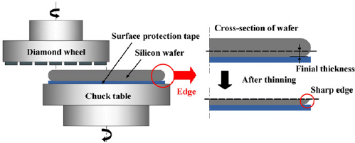
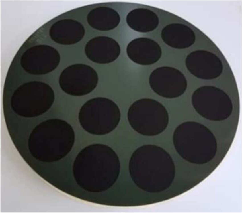
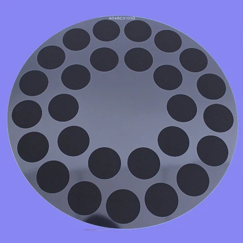
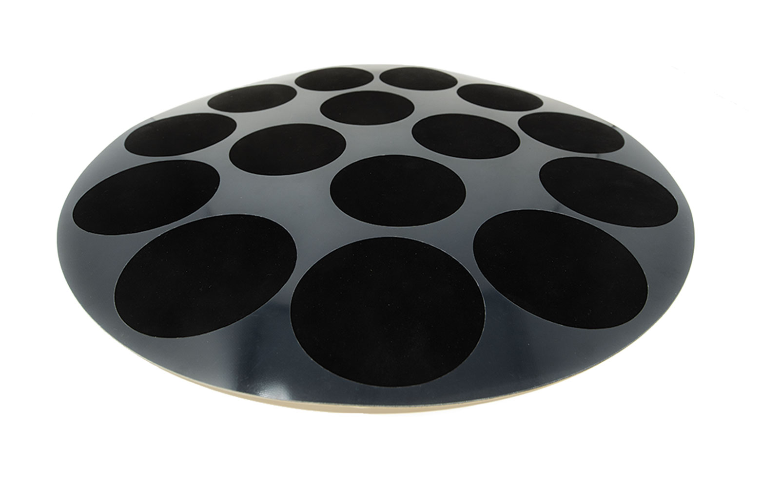
How Polishing Template Edge Design Controls Wafer Edge Profile & Reduces Edge Exclusion

Edge Engineering Guide Every millimeter of edge exclusion zone you eliminate converts directly into additional die area. This guide explains the physics of edge rolloff and the template design parameters ...

By |2026-03-13T09:53:34+08:002026年3月13日|Blog, Industry|0 Comments

Role of Polishing Templates in CMP: How Fixture Design Impacts Wafer Flatness

CMP Process Engineering In chemical mechanical planarization, every nanometer of within-wafer non-uniformity has a device yield consequence. This guide explains exactly how polishing template geometry and backing pad design control ...

By |2026-03-13T09:53:28+08:002026年3月13日|Blog, Industry|0 Comments

FR-4 vs G-10 Fiberglass Polishing Templates: Material Properties & Selection Guide

Material Engineering Guide Two materials. Nearly identical names. Genuinely different performance envelopes. This guide explains exactly when each is the right choice — and when neither is sufficient. By Jizhi ...

By |2026-03-13T09:53:24+08:002026年3月13日|Blog, Industry|0 Comments

Waxless Polishing Templates vs. Wax Mounting: Cost, Quality & Process Comparison

Process Technology Comparison Two fundamentally different approaches to holding a wafer during single-side polishing. One has been the industry standard for decades. The other has largely replaced it — and ...

By |2026-03-13T09:53:19+08:002026年3月13日|Blog, Industry|0 Comments

How to Specify a Polishing Template: 6 Parameters Engineers Must Define

Engineering Specification Guide Incomplete or ambiguous polishing template specifications are the primary cause of first-article failures, TTV excursions, and unnecessary re-qualification cycles. This guide defines each parameter precisely — and ...

By |2026-03-13T09:53:14+08:002026年3月13日|Blog, Industry|0 Comments

Standard vs. Custom Polishing Templates: Which Is Right for Your Wafer Process?

Procurement & Process Decision Guide A structured, engineering-led comparison of cost, lead time, TTV performance, and substrate fit — with a decision framework to guide your next procurement choice. By ...

By |2026-03-13T09:53:08+08:002026年3月13日|Blog, Industry|0 Comments

Polishing Templates for Semiconductor & Silicon Wafer Processing: Complete Guide

Semiconductor Process Equipment Everything engineers, process owners, and procurement teams need to know — from material science and process mechanics to substrate-specific selection and custom engineering. By Jizhi Electronic Technology ...

By |2026-03-13T10:03:30+08:002026年3月13日|Blog, Industry|0 Comments

Custom Polishing Templates for Silicon Wafers – Tailored to Your Carrier Head Specs

Custom Semiconductor Consumables When catalog templates fall short of your TTV, edge profile, or substrate requirements, custom engineering delivers the precision your process demands — from first drawing to production ...

By |2026-03-13T09:50:40+08:002026年3月13日|Blog, Industry|0 Comments

CMP Slurry Storage, Handling & Safety Regulations: Complete EHS Engineering Guide

CMP slurry is not merely a precision chemical — it is a regulated hazardous material in most jurisdictions. H₂O₂-containing slurries are classified as oxidizers under GHS; acidic tungsten slurries are ...

By |2026-03-04T14:56:28+08:002026年3月4日|Blog, Industry|0 Comments

CMP Slurry Filters, Storage & Handling: Complete Engineering Guide

A perfectly formulated CMP slurry can be rendered defective before it ever contacts a wafer — through improper storage temperatures that collapse colloidal stability, contaminated distribution materials that leach metal ...

By |2026-03-04T11:09:39+08:002026年3月4日|Blog, Industry|0 Comments
Go to Top