How to Specify a Polishing Template: 6 Parameters Engineers Must Define
Incomplete or ambiguous polishing template specifications are the primary cause of first-article failures, TTV excursions, and unnecessary re-qualification cycles. This guide defines each parameter precisely — and explains why each one matters.
Why Specification Precision Matters More Than You Might Expect
A polishing template looks deceptively simple: a flat disc with one or more circular holes, bonded to a pad. There are no moving parts, no electronics, no complex chemistry in the material itself. Yet the dimensional precision of a polishing template has a direct, one-to-one relationship with wafer flatness at the nanometer level — the most critical quality attribute in silicon wafer manufacturing and, increasingly, in silicon carbide and compound semiconductor production.
Consider the scale of this relationship. A 10 µm error in work-hole depth — the distance from the backing pad surface to the bottom of the pocket that holds the wafer — translates into a 10 µm systematic TTV error across every wafer polished on that template. At a 300 mm node where the TTV specification may be 1.0 µm or tighter, a 10 µm specification error is not a marginal miss — it is an order-of-magnitude excursion. The template goes directly to scrap, and every wafer polished before the excursion is detected must be re-evaluated.
The same principle applies to every other parameter in the specification. A backing pad hardness that is 10 Shore A units too soft leads to excessive wafer movement and edge rolloff. A carrier plate material specified without confirming slurry pH compatibility leads to progressive delamination, contamination, and dimensional drift over 20–40 polishing cycles. A carrier head geometry assumption that is 0.5 mm wrong on the retaining ring inner diameter produces a template that physically cannot seat in the carrier head.
Understanding the fundamentals of how polishing templates work makes clear why each of these parameters is load-bearing. The six parameters described in this guide are not a bureaucratic checklist — each one controls a distinct failure mode that will manifest in production if the specification is wrong or ambiguous.
The 6 Parameters at a Glance
| # | Parameter | Primary Process Impact | Criticality |
|---|---|---|---|
| P1 | Wafer diameter & final target thickness | TTV, work-hole depth, wafer retention force | Critical |
| P2 | Carrier head model & geometry | Template seating, pressure uniformity, machine fit | Critical |
| P3 | Carrier plate material | Chemical compatibility, template life, contamination risk | Critical |
| P4 | Backing pad type & hardness | Pressure distribution, wafer retention, TTV, edge rolloff | High |
| P5 | Edge enhancement ring requirement | Edge exclusion, edge rolloff, usable die area | High |
| P6 | Cleanroom class & traceability | Particle contamination, quality system compliance | Standard |
The three Critical parameters (P1–P3) define whether the template will physically work in your process at all. An error in any of them produces a template that cannot be used — and must be redesigned and re-fabricated before any process testing can begin. The two High-impact parameters (P4–P5) determine the quality of the polishing result. Errors here produce templates that fit the machine but deliver substandard TTV or edge profiles. P6 governs the cleanroom and documentation standards that your quality system requires; it is rarely a cause of first-article failure but is important for production qualification and ongoing supply.
The 6 Parameters: Full Engineering Specification Guide
Wafer Diameter & Final Target Thickness (FTT)
Sets work-hole diameter and depth — the two most critical dimensionsThese two values are the dimensional foundation of the entire template specification. They directly determine the two most important machined dimensions: work-hole diameter and work-hole depth.
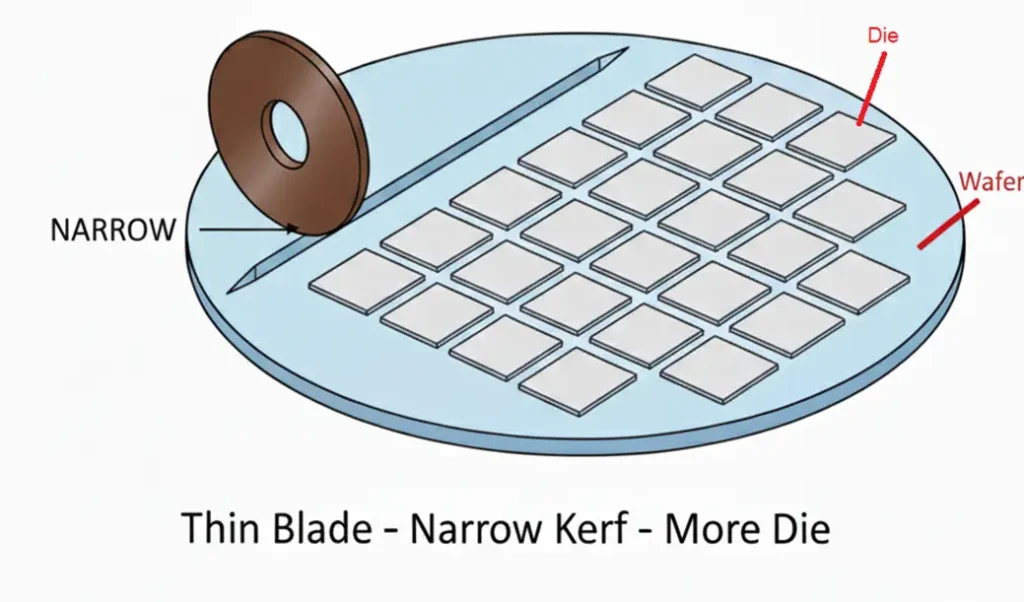
Work-hole diameter is calculated as the wafer OD plus a radial clearance of 0.2–0.5 mm. This clearance is not arbitrary — it must be tight enough to prevent lateral wafer slippage during polishing (which causes scratch defects and non-circular TTV patterns) while loose enough to allow the wafer to seat cleanly into the pocket without stress-induced bow. For 300 mm silicon, a radial clearance of 0.25–0.35 mm is typical. For fragile compound semiconductor substrates (GaAs, InP), tighter clearances of 0.15–0.25 mm are used to reduce lateral movement risk, but require more precise incoming wafer OD control to prevent jamming.
Work-hole depth is the most critical single dimension in the polishing template. It controls the mechanical “stand-off” of the wafer surface relative to the polishing pad contact plane, which directly determines the downforce applied to the wafer under carrier head load. Too deep, and the wafer is recessed below the pad contact plane — polishing pressure is reduced and material removal rate drops, while the edge sees relatively higher pressure, producing edge rollup. Too shallow, and the wafer protrudes above the template surface — edge pressure is reduced and edge rolloff results, with center-high TTV as a secondary effect.
The most common specification error related to FTT is confusing the incoming wafer thickness (before polishing) with the final target thickness (after polishing). Work-hole depth is set against FTT — the thickness of the wafer when it exits the polisher. Specifying work-hole depth against incoming wafer thickness produces a template that is systematically too deep by the material removal amount, which is typically 5–50 µm depending on the process.
Carrier Head Model & Carrier Head Geometry
Defines template outer dimensions, seating fit, and pressure transmission pathThe polishing template must fit precisely within the carrier head’s retaining ring pocket. Get this wrong and the template physically cannot be installed — there is no partial credit for a near-fit geometry. The carrier head information required to specify a template breaks down into three sub-parameters.
Machine platform and carrier head model. Common platforms each have a documented nominal template geometry: Strasbaugh 6EC and 6DS-SP, Peter Wolters AC2000 and AC3000, Speedfam 9B and 9DSP, Lapmaster 20S and 36S, DISCO DAS8830. For well-established platforms with documented catalog templates, the carrier head geometry is known and the template OD, thickness range, and pocket depth are derivable from existing product data. For lesser-known or OEM platforms, a direct measurement of the carrier head pocket is required.
Retaining ring inner diameter. This is the inner diameter of the retaining ring that constrains the template within the carrier head. The template OD must be 0.1–0.3 mm smaller than the retaining ring ID to allow free thermal expansion while preventing lateral play that would shift the template’s work hole(s) out of concentricity with the carrier head axis. Provide this dimension with a tolerance statement — “approximately 300 mm” is not a usable specification.
Carrier head pocket depth. The recess in the carrier head into which the template seats. Template total thickness (carrier plate + backing pad) must be compatible with this pocket depth to ensure the template seats flat, the backing pad is not over-compressed in the unloaded condition, and the retaining ring can be installed and removed without excessive force.
Wafer size: 300 mm
Missing: carrier head model revision, retaining ring ID measurement, pocket depth. “Strasbaugh” has 5+ carrier head configurations for 300 mm — none of which are interchangeable.
Carrier head: Type B (6EC-CB)
Retaining ring ID: 305.5 ± 0.1 mm
Pocket depth: 6.2 ± 0.05 mm
Dimensioned drawing attached. All critical tolerances stated explicitly.
Carrier Plate Material
Must be chemically compatible with slurry pH and temperature across full template service lifeCarrier plate material selection is a chemical engineering decision, not a procurement convenience. The carrier plate is in continuous contact with polishing slurry throughout every polishing cycle. Over time, an incompatible material will swell, delaminate, leach contaminants into the slurry, and change dimensions — all of which degrade process performance and, in severe cases, contaminate the wafer surface.
Three material families cover the vast majority of semiconductor polishing applications. The selection logic follows a simple hierarchy: start with FR-4, step up to G-10 if the slurry is mildly acidic, and specify CXT-grade if the chemistry is outside the laminate envelope entirely. For the detailed material property comparison, our article on FR-4 vs G-10 fiberglass polishing templates covers the full property data.
| Material | pH Range | Typical Application | Key Limitation |
|---|---|---|---|
| FR-4 | 8 – 12 | Si SSP with alkaline silica slurry | Epoxy swells in acid; requires edge sealing to prevent fiber shedding |
| G-10 | 5 – 12 | Si SSP + mildly acidic slurries (citric, HNO₃-buffered) | Not suitable below pH 5; similar fiber-shedding risk if edges unsealed |
| CXT Seamless | 2 – 13 | SiC CMP (KMnO₄), GaAs bromine-based, aggressive oxide CMP | Higher unit cost; custom-only; longer fabrication lead time |
When specifying carrier plate material, do not rely on slurry product names alone — specify the pH range and any oxidant components explicitly. The same slurry brand may be formulated differently for different substrate applications, and supplier formulations change over time. A material selection made against “Cabot Microelectronics SS25” slurry in 2018 may not be valid against the current formulation of the same product.
For SiC CMP applications, the CXT seamless grade is not optional — it is a process requirement. Standard FR-4 templates in KMnO₄ slurry at pH 2–4 typically show visible delamination within 15–25 polishing cycles, followed by progressive slurry penetration into the carrier plate laminate, dimensional swelling, and ultimately work-hole geometry distortion that produces systematic TTV excursions. Full technical guidance on SiC-specific template requirements is in our SiC wafer polishing template guide.
Backing Pad Type & Hardness
Controls pressure distribution uniformity, wafer retention, and edge rolloff tendencyThe backing pad is the mechanical interface between the rigid carrier plate and the wafer backside. Its compliance — the combination of Shore A hardness, thickness, and internal porosity — determines how faithfully the carrier head’s applied pressure is distributed across the wafer area, and how much the wafer is allowed to flex relative to the polishing pad surface.
Specifying backing pad hardness requires knowing three things about your process: the substrate material and its hardness, the nominal carrier head process pressure (in g/cm² or psi), and the target TTV and edge profile requirements. The relationship between these inputs and optimal pad hardness follows a consistent pattern:
- Hard substrates + high process pressure (SiC CMP at 5–7 psi) → hard backing pad (Shore A 70–85). A soft pad would over-compress under high load, reducing effective work-hole depth control and creating TTV instability over the template’s service life as the pad fatigues.
- Soft or fragile substrates at moderate pressure (GaAs, thin Si at 1–3 psi) → soft pad (Shore A 30–55). The soft pad absorbs carrier head pressure non-uniformities and reduces the risk of stress concentrations at the wafer edge that could initiate fracture in brittle III-V materials.
- Standard Si SSP at nominal pressure (2–5 psi) → medium pad (Shore A 55–75). This is the most common configuration and the one for which standard catalog templates are optimized.
Pad thickness matters independently of hardness. Thicker pads provide greater compliance and are preferred for applications where the carrier head has a non-uniform pressure profile (a common characteristic of older or heavily worn carrier heads). Thinner pads provide more precise depth control and are preferred for ultra-tight TTV applications where every micrometer of pad compression must be accounted for.
Edge Enhancement Ring (EER) Requirement
Determines edge exclusion zone and edge rolloff profileThe edge enhancement ring (EER) is an optional but increasingly important feature in polishing templates for advanced process nodes. Its purpose is to modify the pressure distribution in the annular zone between the wafer OD and the work-hole wall — the region that controls edge flatness and determines the size of the edge exclusion zone.
Without an EER, the template in the annular zone adjacent to the wafer edge provides relatively little mechanical support to the polishing pad. The pad deflects slightly under the wafer edge, reducing local contact pressure and creating a characteristic “rolloff” — a zone of lower-than-average material removal rate that leaves the wafer edge thicker than the center. For 300 mm silicon wafers at legacy process nodes, a 3–5 mm edge exclusion zone was standard and acceptable. For advanced logic and memory at 5 nm and below, edge exclusion targets of 1.0–1.5 mm require a polishing template with engineered edge support.
The EER achieves this by adding a precision-machined annular feature on the template back face, concentrically positioned relative to the work hole. This feature increases local stiffness in the edge zone, countering the pad deflection that causes rolloff. The geometry of the EER — inner and outer diameter, height, material — is custom-engineered to the specific wafer diameter, final thickness, backing pad specification, and target edge profile. Read the detailed technical engineering background in our article on edge profile control and edge exclusion reduction.
To specify the EER requirement, provide two inputs: your target edge exclusion in millimeters, and your historical edge profile data (maximum rolloff height at 1 mm and 2 mm from the wafer edge) from your current process. If you have no historical data, the EER geometry is initially estimated from the wafer diameter and backing pad specification, then iterated based on first-article process data.
Cleanroom Class & Traceability Requirements
Governs particle contamination risk and quality system compliancePolishing templates are assembled in a cleanroom environment, and the class of that environment determines the maximum particle population on the template surface at the point of packaging. For most semiconductor production applications, ISO Class 5 (Class 100) assembly is adequate — this is Jizhi’s standard production environment. For advanced front-end-of-line applications at 28 nm and below, where wafer surface particle budgets are extremely tight, ISO Class 4 assembly (10× cleaner than Class 5) may be specified.
Beyond cleanroom class, there are four documentation elements that should be explicitly stated in the specification, as they form the quality system backbone for the template’s entire production life:
- Raw material traceability retention period. Standard Jizhi practice is a minimum of 5 years, covering carrier plate material, backing pad compound, and all adhesive systems. If your quality system or customer audit requirements mandate a longer retention period, specify this explicitly.
- Certificate of Conformance (CoC). A written statement confirming that the delivered lot was manufactured in accordance with the released drawing and all specified quality requirements. This is standard for semiconductor consumable supply; confirm whether your receiving inspection requires a per-lot or per-unit CoC.
- Material certificates. Raw material mill certificates for the carrier plate laminate, confirming composition, dielectric properties, and dimensional conformance to the relevant NEMA or IPC standard. Required for most semiconductor quality audits.
- Per-unit dimensional inspection data. For high-specification applications, a CMM measurement report for each individual template (rather than a sampling-based lot report) may be required. This increases cost and lead time; specify only if your process control requirements genuinely demand it.
5 Common Specification Errors & How to Avoid Them
The following five errors appear repeatedly in polishing template specification submissions. Each has a distinct failure mode and a straightforward prevention method.
Error 1: Confusing Incoming Wafer Thickness with Final Target Thickness
Work-hole depth is set against the final target thickness — the wafer after polishing. Providing the incoming (pre-polishing) wafer thickness produces a template that is systematically too deep, resulting in reduced polishing pressure and a center-thick TTV pattern. Prevention: always label the value you provide as either “incoming thickness before polishing” or “FTT after polishing” — never just “wafer thickness.”
Error 2: Omitting the Work-Hole Depth Measurement Reference Plane
Work-hole depth can be measured from either the backing pad working surface or the carrier plate top face. These differ by the full pad thickness — typically 0.5–1.2 mm. A specification that simply states “work-hole depth: 725 µm” without defining the reference plane is ambiguous and will produce a first-article template that is wrong by the full pad thickness. Prevention: always state “depth from backing pad working surface” or “depth from carrier plate top face” explicitly, and confirm this in writing with the supplier before fabrication begins.
Error 3: Specifying Slurry by Brand Name Without pH Range
Slurry formulations change over time, and the same product name may cover multiple pH variants in a supplier’s portfolio. “We use Cabot SS25” is not a material compatibility specification. Prevention: always state the pH range and any oxidant components (H₂O₂, KMnO₄, NH₄OH, HF, etc.) explicitly. This is the information your template supplier needs to validate material selection — the slurry brand name alone is insufficient.
Error 4: Assuming Carrier Head Geometry from Machine Platform Name
Multiple carrier head configurations exist for most major polishing platforms, and template geometry differs between them. A Strasbaugh 6EC with a Type A carrier head and a Strasbaugh 6EC with a Type B head require different templates. Prevention: provide the carrier head model designation, not just the machine platform name. If the carrier head type is unknown, measure the retaining ring ID and pocket depth directly and provide the raw measurements with a tolerance statement.
Error 5: Specifying Backing Pad as “Standard” Without Hardness
Different suppliers use different backing pad compounds as their “standard” — and even within a single supplier, standard pad hardness may be optimized for different wafer diameters. A 300 mm standard pad and a 150 mm standard pad are often different compounds with different Shore A values. Prevention: always specify backing pad hardness by Shore A range (e.g., “Shore A 60–70”) and nominal thickness. If you do not know what hardness your current template uses, ask your current supplier for the specification before switching.
Pre-Order Specification Checklist
Use the following checklist before submitting a polishing template specification to Jizhi or any other supplier. Each item corresponds to a parameter that, if missing or ambiguous, will generate an engineering clarification request and extend your lead time.
- Wafer diameter (mm): state the nominal OD with tolerance if non-standard
- Final target thickness after polishing (µm): confirm this is FTT, not incoming thickness
- Work-hole count and pattern: single-cavity or multi-cavity; if multi, specify count
- Polishing machine model: manufacturer + model + carrier head type designation
- Retaining ring inner diameter (mm): measured value with tolerance, not nominal guess
- Carrier head pocket depth (mm): or provide a dimensioned drawing of the carrier head
- Slurry type and pH range: include oxidant components if present
- Process temperature: state if above 40°C
- Carrier plate material: FR-4, G-10, or CXT; or request a material recommendation
- Backing pad Shore A hardness range and nominal thickness (mm): do not leave as “standard”
- Edge enhancement ring required? (Yes/No): if Yes, provide edge exclusion target and historical edge profile data if available
- Cleanroom assembly class: ISO 5 standard, or ISO 4 if required
- Documentation requirements: CoC, material certificates, per-lot or per-unit CMM report
- Quantity: qualification lot size and anticipated production lot size
- Target ship date or required-by date: for lead time planning