Standard vs. Custom Polishing Templates: Which Is Right for Your Wafer Process?
A structured, engineering-led comparison of cost, lead time, TTV performance, and substrate fit — with a decision framework to guide your next procurement choice.
The Right Question to Ask First
Every semiconductor fab running a single-side polishing process will eventually face this procurement decision: do we qualify a standard catalog polishing template, or do we engage a supplier for a custom-engineered solution? The framing of this question matters. It is not fundamentally a cost question, nor a lead-time question — although both are real considerations. It is first and foremost a process requirements question.
The right starting point is not “which is cheaper?” but rather: can a standard template meet my process specifications with acceptable risk? If the answer is yes, the standard path is almost always faster, cheaper, and lower-risk. If the answer is no — or “probably, but we’re not sure” — then custom engineering moves from being a premium option to a process necessity.
This article provides the structured comparison and decision framework to answer that question rigorously, covering the full lifecycle from initial procurement to production supply. For a deeper understanding of the technical foundations that drive this decision, our complete polishing templates guide provides the engineering context.
What Standard Polishing Templates Include
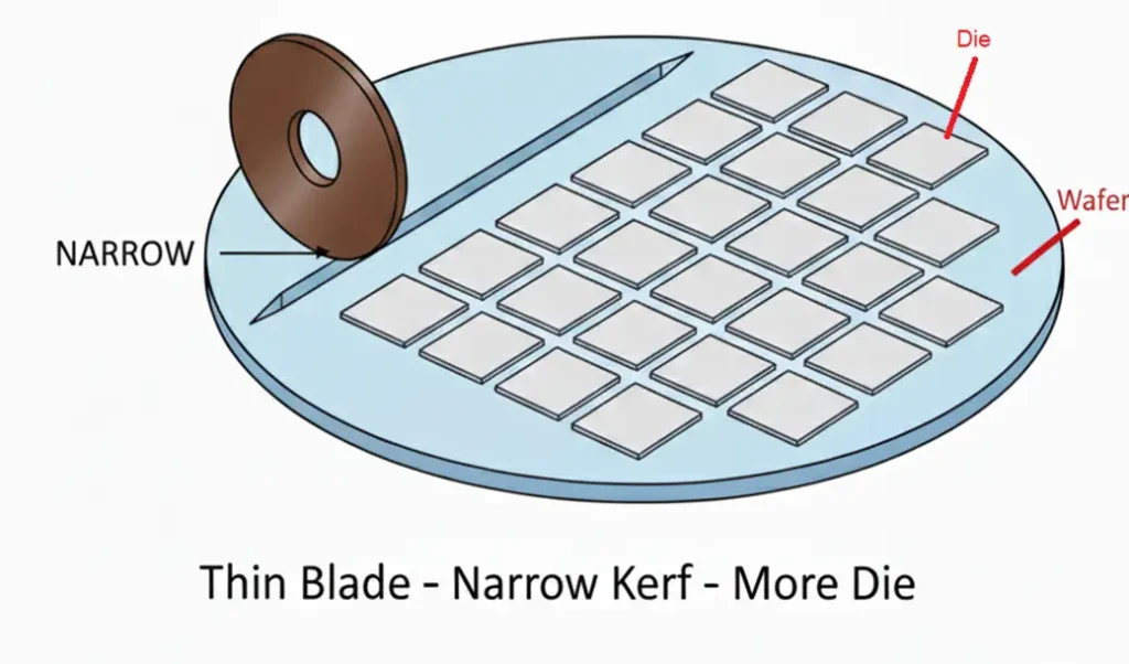
Standard polishing templates are catalog products manufactured to fixed, published specifications covering a defined set of wafer diameters (most commonly 100 mm, 150 mm, 200 mm, and 300 mm), carrier head platforms (Strasbaugh, Peter Wolters AC Series, Speedfam, Lapmaster), and material grades (FR-4, G-10). They are produced in volume against stable, release-controlled drawings, and are available from stock or on short lead times.
The term “standard” does not imply “low performance.” For the applications they are engineered for, standard templates from a quality manufacturer deliver reliable, repeatable TTV results that satisfy the majority of silicon prime and test wafer polishing requirements. The key word is for the applications they are engineered for — which brings us to the limits of the standard template’s fit envelope.
Standard templates are defined by three fixed constraints:
- Fixed geometry: Work-hole diameter, depth, count, and pattern are as-cataloged. Carrier plate OD, thickness, and any keying features match the target machine platform exactly — which means they only fit that platform.
- Fixed material grade: Standard templates are produced in FR-4 or G-10; CXT-grade chemically resistant materials are typically custom-only, because the number of applications requiring them is too diverse to standardize.
- Fixed backing pad specification: Standard templates carry a single backing pad specification validated against the most common process conditions for that diameter. Departures from those conditions — higher pressure, different slurry, thinner target wafer — may fall outside the pad’s validated performance envelope.
What Custom Polishing Templates Offer
Custom polishing templates are engineered from a blank-sheet specification to match your exact carrier head geometry, wafer final target thickness, substrate material, slurry chemistry, and process performance requirements. Every critical dimension — work-hole depth, carrier plate bow tolerance, backing pad hardness and thickness, edge enhancement ring geometry — is determined by your process parameters rather than a catalog constraint.
Custom engineering does not simply mean “non-standard dimensions.” It means that the template has been designed as a system, with all parameters chosen in coordination rather than inherited from a fixed product definition. The result is a template that is optimized for your specific process conditions rather than for the broadest common denominator of a market segment.
The trade-off is time and process investment. A custom template requires a specification intake, a design review, first-article fabrication, and a process qualification before it enters production supply. This takes 4–8 weeks from initial specification to first production-qualified lot — significantly longer than pulling a standard template from stock. After qualification, however, repeat supply lead times converge with standard template supply timelines. For the full custom engineering workflow, see our article on custom polishing templates for silicon wafers.
Head-to-Head Comparison
Performance Scorecard by Category
The head-to-head comparison above captures the binary advantages and disadvantages. The scorecard below provides a more nuanced view of relative performance across the dimensions that matter most in a procurement decision, rated on a five-point scale for typical applications.
Total Cost of Ownership: Beyond Unit Price
Unit price is the most visible cost difference between standard and custom polishing templates, but it is frequently the least important factor in a properly scoped total cost of ownership (TCO) analysis. The following framework captures the full cost picture across a 12-month production period, illustrating why custom templates often deliver lower effective cost per polished wafer in advanced or high-specification applications — despite higher unit prices.
| Cost Element | Standard Template | Custom Template | Notes |
|---|---|---|---|
| Unit purchase price | Baseline (1.0×) | 1.2×–1.6× baseline | Custom premium varies by geometry complexity |
| NRE / engineering fee | None | $0–$2,000 (one-time) | Amortized over production volume; often waived for standard geometry variants |
| Qualification wafer cost | Low (1–2 lots) | Moderate (2–4 lots) | Custom may require additional qualification lots if first-article iteration needed |
| Yield loss from TTV excursions | Higher risk if spec is marginal | Lower — optimized to process | Even 0.1% yield improvement on 300 mm prime wafers offsets significant template cost premium |
| Template replacement frequency | Standard cycle life | Often extended | Custom CXT-grade templates in SiC applications can last 2–3× longer than standard FR-4 |
| Downtime from process excursions | Higher risk (marginal fit) | Lower (optimized fit) | Polisher downtime for investigation and re-qualification is a significant hidden cost |
| Effective cost per polished wafer | Lower for standard Si SSP | Lower for advanced / non-Si | Breakeven point shifts with wafer value and process specification stringency |
* Cost multiples are indicative. Actual figures depend on wafer diameter, material grade, order volume, and specific application requirements. Request a formal quotation for application-specific cost modeling.
Decision Framework: 5 Questions to Guide Your Choice
The following five questions lead to a well-reasoned procurement decision for the majority of polishing template applications. Work through them in order — an early “custom required” answer makes subsequent questions less relevant.
Common platforms (Strasbaugh, Peter Wolters, Speedfam) at 150–300 mm Si are typically covered. Verify carrier head model compatibility before assuming catalog fit.
Non-catalog carrier head geometry, non-standard wafer OD, or multi-pocket configurations for small diameters all require custom engineering. No further evaluation needed.
Standard FR-4 templates are chemically compatible. Material selection is not a disqualifying factor.
SiC, GaAs, or acidic slurry chemistries (pH <5) require CXT-grade material — only available in custom configurations. Review our material guide for pH compatibility details.
Standard templates are typically validated to 1.0–2.0 µm TTV for well-maintained processes. Your target is within standard territory.
TTV targets below 1.0 µm require tight carrier plate bow specification (≤5 µm) and optimized backing pad uniformity — typically only achievable through custom engineering. Catalog templates may pass initial qualification but show lot-to-lot TTV drift.
Standard template edge geometry is adequate for edge exclusion ≥ 2 mm in most silicon SSP applications.
Edge exclusion targets below 2 mm, or persistent edge rolloff in your current process, indicate a need for edge enhancement ring (EER) design. Standard templates do not offer this feature. See our article on edge profile control for engineering details.
If you have answered YES to all previous questions and can accept the custom lead time, evaluate on total cost of ownership. For advanced Si or tight-spec applications, custom will typically deliver better long-run economics.
Use a standard template to meet immediate production demand while simultaneously initiating a custom qualification program. This is the most common approach for engineering-driven process improvements.
Scenarios Where Standard Templates Are the Correct Choice
Despite the performance advantages of custom engineering for many applications, standard polishing templates are the right choice — and sometimes the only practical choice — in a well-defined set of circumstances.
New Process Development and Early R&D
When a polishing process is in early development, the process parameters are unstable and the specification targets are provisional. Committing to a custom template design at this stage locks in geometry choices that may need to change as the process matures. Standard templates provide a stable, well-characterized baseline from which process development can proceed, with custom optimization deferred until the process is approaching production readiness. This approach also eliminates the risk of custom template re-engineering costs when process parameters are revised mid-development.
Emergency or Unplanned Stock-Outs
Semiconductor fabs occasionally face unplanned consumable stock-outs due to supply chain disruptions, demand spikes, or unexpected template wear acceleration. In these situations, standard templates available from stock are the only viable short-term solution. A well-managed consumable inventory program — discussed in our article on polishing template lifespan and replacement planning — includes standard template safety stock to protect against custom supply interruptions.
High-Volume Commodity Silicon Polishing
For commodity silicon wafer production at 200 mm and 300 mm where the TTV target is in the 1.5–3.0 µm range, the incremental TTV improvement achievable through custom engineering does not generate sufficient yield recovery to offset the custom premium at high volumes. Standard templates at scale typically offer the lowest effective cost per polished wafer for commodity specifications.
Evaluation and Benchmarking
When evaluating a new polishing machine platform or benchmarking polishing performance against a known reference, starting with a validated standard template removes template variability from the experiment. Once the machine baseline is established, custom templates can be introduced as a controlled process variable.
Scenarios Where Custom Templates Deliver Decisive Advantages
Silicon Carbide (SiC) and Compound Semiconductor Polishing
This is the clearest case for custom engineering. SiC CMP with KMnO₄-based slurry at pH 2–4 is chemically incompatible with standard FR-4 templates. Delamination, dimensional instability, and slurry contamination from carrier plate material degradation are consistently observed within 10–20 polishing cycles on standard templates in this environment. CXT-grade custom templates solve the chemistry problem entirely and deliver template lives of 50–100+ cycles in production SiC applications. The economic case is unambiguous. Read the full technical analysis in our dedicated guide to SiC wafer polishing templates.
Advanced Logic and Memory Applications (<1.0 µm TTV)
Leading-edge device fabrication at 5 nm node and below imposes TTV requirements that standard templates struggle to meet consistently across production lots. Lot-to-lot variation in standard catalog templates — arising from raw material variability in FR-4/G-10 dielectric properties and backing pad compound batches — produces TTV excursions that are difficult to distinguish from process drift. Custom templates with tighter incoming material specifications and per-lot CMM inspection provide the dimensional consistency that advanced silicon applications require.
Legacy or OEM Machine Platforms
Semiconductor fabs frequently run legacy polishing machines that predate current catalog standards, or machines from OEM manufacturers whose carrier head geometries are not covered by any standard catalog. For these platforms, custom engineering is not a performance optimization — it is the only procurement path available.
Tight Edge Exclusion Requirements
As device layouts push closer to the wafer edge to maximize die yield, the 3 mm edge exclusion that was standard for 200 mm silicon in the early 2000s has given way to 1.5 mm and 1.0 mm requirements on advanced 300 mm processes. Standard templates without edge enhancement ring (EER) features cannot reliably achieve sub-2 mm edge exclusion. Custom EER-integrated templates — designed to the exact edge profile specification of the device layer — provide the edge flatness control that advanced process nodes require. Our article on edge profile and edge exclusion control covers the engineering design principles in detail.
The Hybrid Approach: Standard Today, Custom Tomorrow
In practice, many semiconductor manufacturers use a hybrid strategy that captures the speed and cost advantages of standard templates while building toward the performance benefits of custom engineering. The typical sequence looks like this:
- Production launch with standard templates. Get the process running quickly using catalog products. Establish baseline TTV, edge profile, and template cycle life data under production conditions.
- Collect process data. Run 3–6 months of production with systematic SPC monitoring of TTV, SFQR, and edge profile. Identify which performance gaps, if any, are consistently template-related versus other process variable contributions.
- Submit custom engineering specification based on real data. Use the baseline production data — not engineering estimates — to define the custom template specification. Work-hole depth, backing pad hardness, and EER geometry are all specified against measured process performance rather than theoretical targets.
- Qualify custom template in parallel with standard supply. Run the custom template qualification while standard template production continues uninterrupted. This eliminates any supply risk during the qualification period.
- Transition fully to custom once qualified. Maintain standard template safety stock for emergency coverage. Review the custom template specification annually as the process evolves.
The hybrid approach is particularly well-suited to SiC and compound semiconductor applications entering production scale-up, where the process is still maturing but the chemical incompatibility of standard templates is a known risk. Start with the best-available standard template for the chemistry, collect failure mode data, and design the first custom CXT-grade template against confirmed field failure data rather than theoretical compatibility concerns alone.
Switching Between Standard and Custom: What You Need to Know
Whether transitioning from standard to custom or returning from custom to standard in a supply disruption scenario, the change management process is the same: any template change is a process change and must be treated accordingly under your quality management system.
Qualification Scope for Template Changes
The scope of re-qualification depends on the degree of change. A custom template designed as a dimensional drop-in replacement for an existing standard template — identical carrier plate OD, thickness, and backing pad spec, only differing in work-hole depth by 5 µm — may qualify on a single lot with statistical comparison to the existing baseline. A template with new material grade (FR-4 to CXT), different backing pad hardness, or added EER geometry constitutes a larger process change and typically requires 3–5 qualification lots with full TTV, SFQR, and edge profile characterization.
Traceability and Change Control
Document the template transition under your engineering change order (ECO) system. Key documentation to capture includes the Jizhi part number and revision of both the outgoing and incoming template, lot numbers used during qualification, baseline and post-change TTV and edge profile data, and any process recipe adjustments made in response to the template change. This documentation becomes critical if a yield excursion occurs weeks or months after the transition, when the template change may not be immediately obvious as a candidate root cause.
Maintaining consistent contamination control practices through any template transition is equally important — our guide to contamination control in polishing templates outlines the handling and storage protocols that apply regardless of template type.