logo

Über semiconductor

Dieser Autor hat noch keine Angaben gemacht.
Bislang hat semiconductor 51 Blogeinträge erstellt.

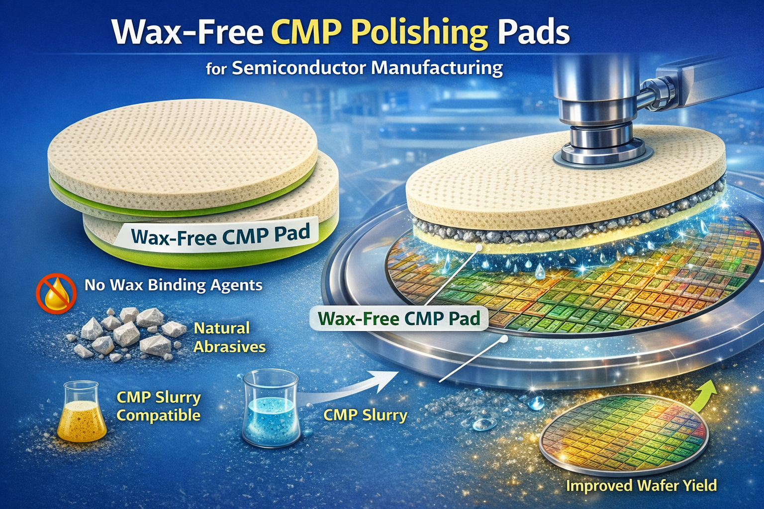
CMP-Polierpads - Materialien und Aufbau erklärt

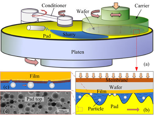
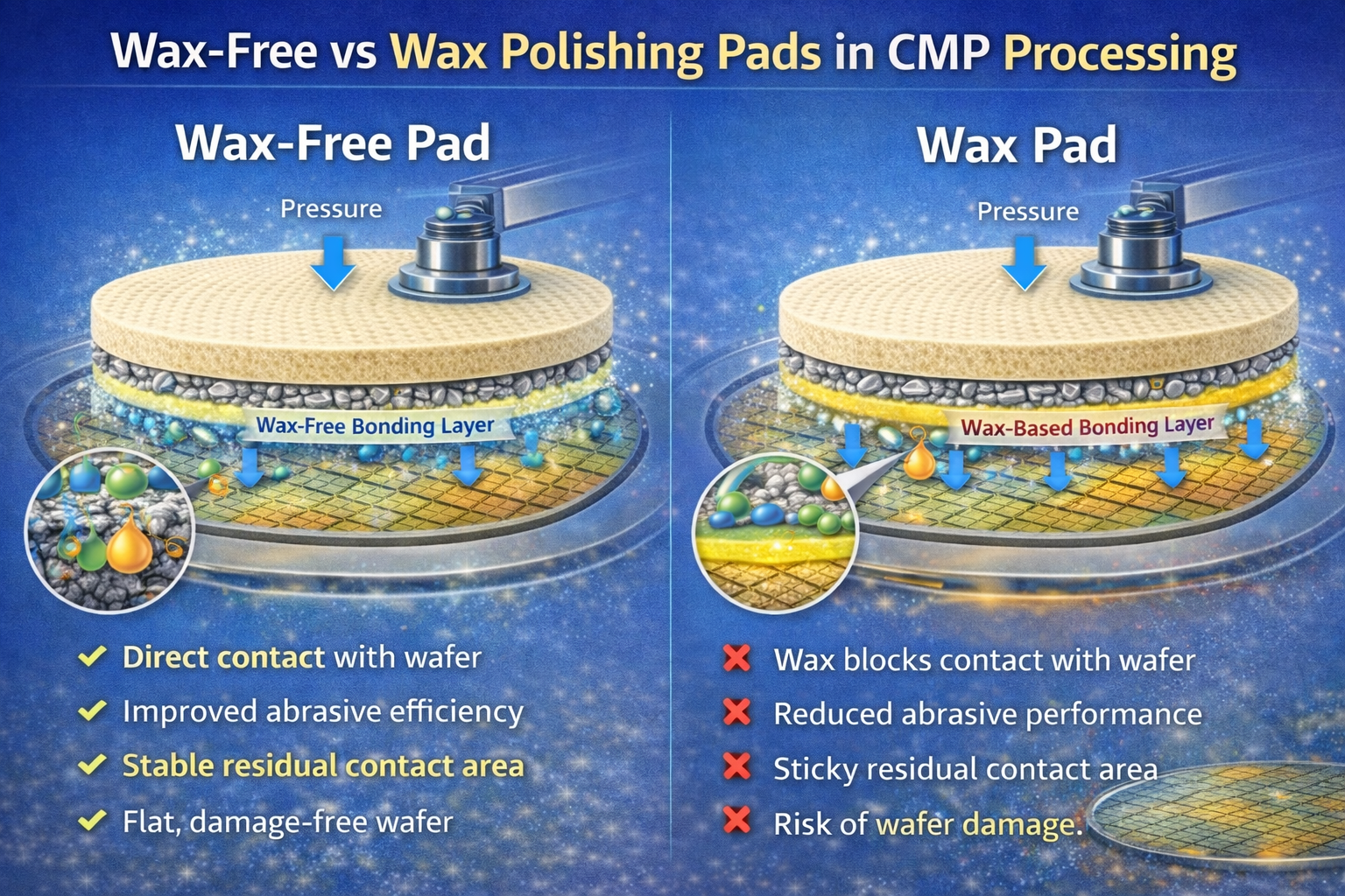
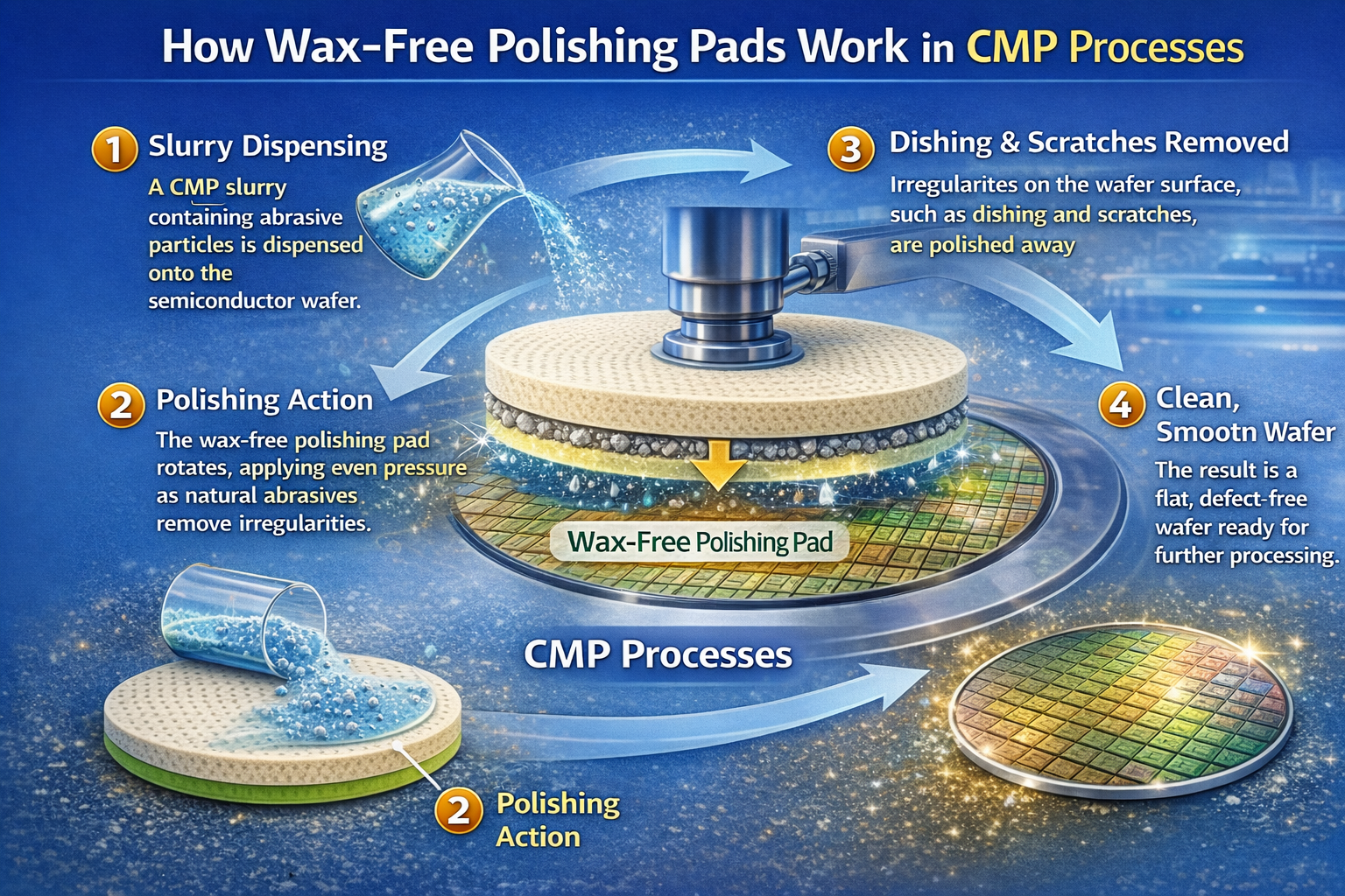
Bei der CMP bestimmen die Materialien der Polierpads die grundlegenden mechanischen, chemischen und tribologischen Wechselwirkungen, die letztendlich die Planarisierungseffizienz, die Fehleranfälligkeit und die Prozessstabilität bestimmen. Bei wachsfreien CMP-Polierpads ist die Materialauswahl sogar noch kritischer, da die Fixierung des Wafers, die Kraftübertragung und die Interaktion mit dem Schlamm direkt von der Masse und den Oberflächeneigenschaften des Pads und nicht von zusätzlichen Wachsschichten bestimmt werden. Dieses Dokument bietet eine Analyse der CMP-Polierpad-Materialien auf der Ebene der Materialmechanismen und konzentriert sich dabei auf Polymersysteme, mikrostrukturelles Design, mechanische Parameter, Verschleißverhalten und ihre spezifischen Auswirkungen auf wachsfreie Pad-Architekturen. Inhaltsverzeichnis Überblick über CMP-Polierpad-Materialien Polymerchemie und Matrixdesign Mikrostruktur und ...

Von |2026-01-12T10:54:52+08:002026年1月12日|Blog, Industrie|0 Kommentare

Wachsfreie Polierpads in CMP-Prozessanwendungen

In der modernen Halbleiterfertigung ist CMP kein isolierter Arbeitsschritt mehr, sondern ein eng integriertes Prozessmodul, das mit der vorgelagerten Abscheidung, der nachgelagerten Reinigung und dem allgemeinen Ertragsmanagement interagiert. Die Einführung von wachsfreien CMP-Polierpads verändert die Art und Weise, wie Wafer gehalten, geladen, poliert und freigegeben werden, grundlegend und erfordert eine bewusste Prozessintegration statt eines einfachen Ersatzes von Verbrauchsmaterialien. Dieses Dokument konzentriert sich darauf, wie wachsfreie Polierpads praktisch in CMP-Prozesse integriert werden, welche Prozessparameter direkt betroffen sind und wie Fabs wachsfreie Architekturen nutzen können, um Prozessstabilität, Ausbeutekonsistenz und Kosteneffizienz zu verbessern. Inhaltsverzeichnis Integration von wachsfreien Pads in CMP-Prozesse ...

Von |2026-01-12T10:53:59+08:002026年1月12日|Blog, Industrie|0 Kommentare

Wax-Free vs Wax Polishing Pads in CMP Processing

In chemical mechanical planarization (CMP), the polishing pad is not merely a consumable surface but a critical process component that directly affects wafer flatness, material removal rate (MRR), defectivity, yield stability, and overall cost of ownership (CoO). Among available pad architectures, wax-free CMP polishing pads and traditional wax-based polishing pads represent two fundamentally different philosophies of wafer fixation, force transmission, and contamination control. This page provides an engineering-level comparison between wax-free and wax polishing pads, focusing on structural design, adsorption mechanisms, process behavior, defect risks, maintenance complexity, and long-term manufacturing economics. The goal is to support data-driven decision-making rather than ...

Von |2026-01-12T10:49:50+08:002026年1月12日|Blog, Industrie|0 Kommentare

How Wax-Free Polishing Pads Work in CMP Processes

    Table of Contents 1. Introduction: Why Wax-Free Pad Working Principles Matter 2. CMP System Context: Wax-Free Pads as a Mechanical Subsystem 3. Pad–Wafer Contact Mechanics Without Wax Bonding 4. Wafer Loading and Initial Adsorption Formation 5. Pressure Ramp-Up and Adsorption Force Stabilization 6. Slurry Introduction and Frontside–Backside Decoupling 7. Steady-State CMP: Dynamic Adsorption Under Motion 8. Thermal and Mechanical Stability During CMP Operation 9. Controlled Wafer Release and De-Adsorption Behavior 10. Manufacturing-Level Process Control Implications 1. Introduction: Why Wax-Free Pad Working Principles Matter Understanding how wax-free polishing pads work is essential for modern CMP process development because wafer ...

Von |2026-01-12T10:42:02+08:002026年1月12日|Blog, Industrie|0 Kommentare

Wax-Free Adsorption Polishing Pad Technology

  Table of Contents 1. Technology Overview: Adsorption as a Replacement for Wax Bonding 2. Fundamental Sources of Adsorption Force in Wax-Free Pads 3. Pad Microstructure Design and Adsorption Efficiency 4. Contact Mechanics at the Pad–Wafer Interface 5. Tunable Engineering Parameters Affecting Adsorption 6. Adsorption Stability Under CMP Operating Conditions 7. Adsorption Degradation and Failure Modes 8. Position of Adsorption Technology Within CMP Systems 1. Technology Overview: Adsorption as a Replacement for Wax Bonding Wax-free adsorption polishing pad technology was developed to eliminate the inherent limitations of wax-based wafer bonding in CMP. Traditional wax layers introduce viscoelastic behavior, thermal sensitivity, ...

Von |2026-01-12T10:48:33+08:002026年1月12日|Blog, Industrie|0 Kommentare

Wax-Free CMP Polishing Pads for Semiconductor Manufacturing

  Table of Contents 1. Definition and Technical Scope of Wax-Free CMP Polishing Pads 2. Product Forms and Design Intent of Wax-Free Polishing Pads 3. Core Technology: Wax-Free Adsorption Fundamentals 4. How Wax-Free CMP Polishing Pads Work in Practice 5. Wax-Free vs Wax-Based CMP Polishing Pads 6. Integration of Wax-Free Pads in CMP Processes 7. Material and Structural Foundations of Wax-Free CMP Pads 1. Definition and Technical Scope of Wax-Free CMP Polishing Pads Wax-free CMP polishing pads are engineered wafer holding and polishing interfaces designed to operate without wax or adhesive bonding layers during chemical mechanical planarization. Unlike traditional wax-based ...

Von |2026-01-12T10:46:47+08:002026年1月12日|Blog, Industrie|0 Kommentare

How to Choose CMP Slurry

  An Engineering-Level Decision Framework for Semiconductor Wafer Polishing Table of Contents 1. Introduction 2. First-Principles Approach to Slurry Selection 3. Wafer Material Considerations 4. Matching Slurry Type to CMP Process 5. Key Performance Metrics 6. Process Window & Margin Engineering 7. Compatibility with CMP Polishing Pads 8. Defectivity & Yield Risk Assessment 9. CMP Tool & Delivery System Constraints 10. High-Volume Manufacturing (HVM) Considerations 11. Common CMP Slurry Selection Mistakes 12. Qualification & Ramp-Up Strategy 13. Engineering Summary 1. Introduction Choosing the right CMP slurry is one of the most consequential decisions in semiconductor manufacturing. Unlike many consumables, slurry ...

Von |2026-01-05T16:34:14+08:002026年1月5日|Blog, Industrie|0 Kommentare

CMP Slurry Filters

  Filter Media, Housing Design, and Point-of-Use Control in Semiconductor CMP Table of Contents 1. Overview of CMP Slurry Filters 2. Role of Filters in CMP Yield Control 3. Filter Media Materials 4. Absolute vs Nominal Rating 5. Pore Size Distribution & Cutoff Behavior 6. Filter Housing Design 7. Point-of-Use (POU) Filtration 8. Chemical Compatibility & Extractables 9. Performance Data & Lifetime Modeling 10. Failure Modes & Root Cause Analysis 11. HVM Filter Management Strategy 12. How to Select CMP Slurry Filters 13. Future Trends 1. Overview of CMP Slurry Filters CMP slurry filters are precision components designed to remove ...

Von |2026-01-05T16:28:13+08:002026年1月5日|Blog, Industrie|0 Kommentare

CMP Slurry Filtration

  Particle Control, Yield Protection, and Process Stability in Semiconductor CMP Table of Contents 1. Introduction 2. Why Filtration Is Critical in CMP 3. Particle Sources in CMP Slurry Systems 4. Particle Size vs Defect Mechanisms 5. CMP Slurry Filter Technologies 6. Filter Pore Size Selection Strategy 7. Chemical Compatibility & Slurry Stability 8. Experimental Data & Filtration Performance 9. Filtration Process Window 10. Integration with CMP Tools 11. Filtration Failure Modes & RCA 12. HVM Filtration Strategy 13. Future Trends 1. Introduction CMP slurry filtration is one of the most underestimated yet yield-critical elements in semiconductor manufacturing. While slurry ...

Von |2026-01-05T16:25:16+08:002026年1月5日|Blog, Industrie|0 Kommentare

Tungsten CMP Slurry for Semiconductor Manufacturing

  Table of Contents 1. Introduction to Tungsten CMP 2. Tungsten CMP Applications in Semiconductor Devices 3. Material Properties of Tungsten Relevant to CMP 4. Chemical–Mechanical Removal Mechanism 5. Tungsten CMP Slurry Composition Architecture 6. Chemical Kinetics & Rate-Limiting Steps 7. Engineering Parameters & Experimental Data 8. Process Window & Control Maps 9. Defect Mechanisms & Root Cause Analysis 10. High-Volume Manufacturing Challenges 11. Slurry Selection & Optimization Guidelines 12. Future Trends in Tungsten CMP Slurry 1. Introduction to Tungsten CMP Tungsten Chemical Mechanical Planarization (CMP) plays a critical role in semiconductor manufacturing, particularly for contact plug and via fill ...

Von |2026-01-05T16:19:16+08:002026年1月5日|Blog, Industrie|0 Kommentare
Nach oben gehen