Wafer Dicing Process Step by Step Guide for Engineers
← Back to: Diamond Dicing Blades: The Complete Guide
Wafer dicing — the process of singulating a finished wafer into individual die — sits at the intersection of mechanical precision, material science, and process control. A single parameter set too aggressively can wipe out yield gains earned upstream in fab. This guide walks through the complete dicing workflow from wafer preparation to post-dice inspection, with engineering-level detail on setup, parameters, and the decisions that separate high-yield processes from troublesome ones.
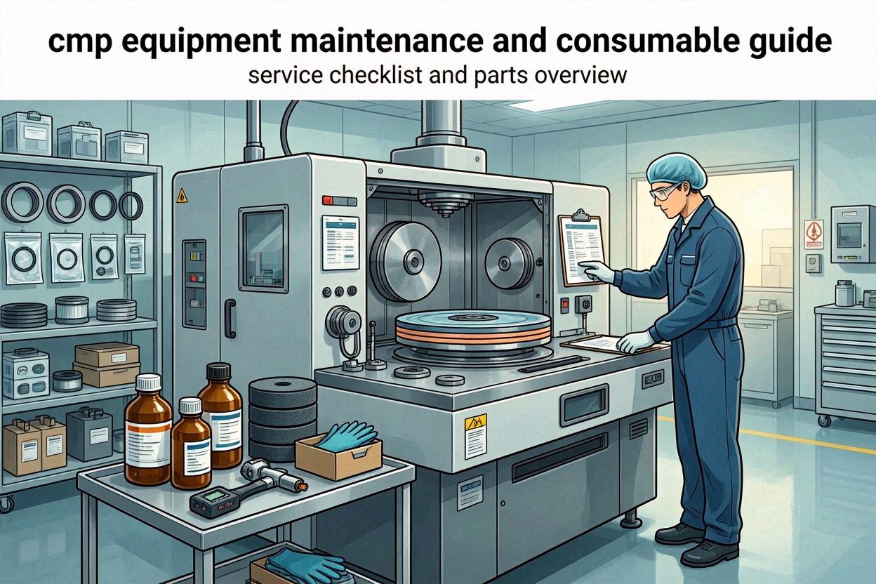
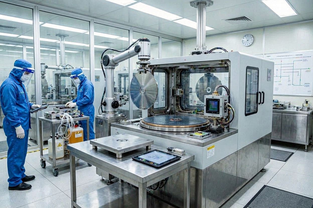
1. Process Overview and Equipment
Wafer dicing typically takes place in the back-end-of-line (BEOL) assembly area, after wafer fabrication and electrical testing are complete. The core equipment is a dicing saw — a precision machine comprising a high-speed spindle (typically 10,000–60,000 RPM), a vacuum chuck stage that holds the wafer frame, an alignment vision system, and a coolant delivery system. Major saw platforms used globally include the DISCO DAD series, K&S 982 series, and ACCRETECH TSK series.
The dicing blade — the consumable diamond cutting tool mounted on the spindle — is the process element with the most direct impact on yield and die quality. Blade selection principles are covered in depth in our complete dicing blade guide and the dedicated bond type comparison. This article focuses on the process workflow around the blade, not blade selection itself.
There are two primary dicing modes in common use:
- Single-pass dicing: One blade makes a full-depth cut through the wafer in a single pass. Simpler setup; suitable for most standard applications.
- Step-cut dicing (dual-spindle): A wider blade (Z1 spindle) makes a partial-depth first cut, and a thinner blade (Z2 spindle) completes the singulation. Used when both top-surface and back-surface chipping must be tightly controlled simultaneously.
Step 1 — Backside Grinding and Wafer Thinning
Before dicing, most production wafers are thinned from their as-grown thickness (typically 725–775 µm for 200 mm and 300 mm Si wafers) to the target die thickness. This is performed by a backside grinding (BSG) machine, which uses a diamond grinding wheel to remove material from the wafer’s non-device side. Target thicknesses range from 300 µm for standard logic die down to 50 µm or less for thin die used in stacked packages.
The post-grind wafer surface quality matters for dicing: sub-surface damage from coarse grinding can propagate into die body cracks during the cutting step. A two-step grinding process — rough grind followed by fine grind — minimises sub-surface damage depth. Some processes add a stress relief step (chemical etch, plasma, or CMP polishing) after grinding to remove the damaged layer entirely before dicing.
Step 2 — Tape Mounting (Frame Lamination)
After thinning, the wafer is laminated onto a dicing frame tape mounted in a metal or plastic ring frame. The tape holds the individual die in position after singulation, allowing them to be transported as an array and picked up individually by downstream die-attach equipment.
Tape Type Selection
Tape selection depends on the die-attach process used downstream:
- UV-release tape: Adhesion is strong during dicing, then reduced by UV exposure to allow easy die pick-up. Most common for standard Si dicing.
- Thermal-release tape: Releases adhesion at elevated temperature. Used in some LED and compound semiconductor applications.
- Standard (non-release) tape: Used where die ejection forces are high enough that reduced adhesion is not required.
Tape thickness is a direct input to the blade exposure calculation. Measure actual tape thickness with a micrometer and use this value in the exposure formula:
Exposure = Wafer thickness + Tape thickness + 0.05–0.10 mm clearance
Tape lamination must be performed without air bubbles or wrinkles under the wafer — both create local variations in blade load that cause intermittent chipping. Lamination temperature and pressure should be set per the tape manufacturer’s specification.
Step 3 — Blade Selection and Installation
With wafer thickness and tape type confirmed, select the dicing blade based on substrate material, required kerf width, and chipping specification. The full selection framework is described in the material compatibility chart y specifications guide.
Installation Checklist
- Verify blade OD, ID (bore), thickness, and bond type match the process specification.
- Inspect blade for visible damage — cracks, edge chips, or deformed hub before mounting.
- Clean the spindle flange faces with lint-free cloth and isopropyl alcohol; verify no debris on contact surfaces.
- Mount blade per flange type (hub type: seat hub face flat against inner flange; hubless: sandwich between matched flanges). See our hub vs. hubless guide for detailed installation steps.
- Tighten retaining nut to the torque value specified in the saw manual — do not over-tighten (can warp thin blades) or under-tighten (blade can shift during cutting).
- Check blade runout (TIR) — acceptable value is typically ≤2 µm for standard applications, ≤1 µm for fine-pitch.
Step 4 — Spindle Warm-Up and Initial Blade Dressing
Before cutting production wafers, the spindle must reach thermal equilibrium. At startup, the spindle bearings and shaft are at ambient temperature; as the spindle accelerates to operating speed, friction heats the bearing assembly and causes thermal expansion of the shaft. This expansion shifts the blade’s axial position and increases runout until steady-state temperature is reached — typically after 5–10 minutes of idle spinning at operating RPM.
Skipping warm-up is a common source of elevated chipping on the first few wafers of a production run, as the blade geometry is still drifting during these cuts. Always include a documented warm-up step in your process traveller.
A new blade also requires initial dressing before cutting production wafers. The manufacturing process leaves diamond grains partially buried in the bond matrix; an initial dress pass on a dedicated dresser board exposes the cutting surface and conditions the blade geometry. Typically 5–20 dress passes at moderate feed rate are sufficient. Full dressing procedures are described in our blade dressing tutorial.
Step 5 — Alignment and Kerf Check
With the blade installed, warmed up, and dressed, load a test wafer (or a scrap wafer of the same material and thickness) and perform the following alignment checks:
- Die layout alignment: The saw’s vision system identifies the wafer street pattern and aligns the cutting path to the scribe lines. Verify alignment accuracy by checking the offset between the programmed cut line and the actual street centre under the microscope — target is typically ≤2 µm offset.
- Cut depth verification: Make a single test cut and inspect the tape underside to confirm the blade has penetrated fully through the wafer and tape backing without cutting into the tape frame.
- Kerf width measurement: Measure the actual kerf width under the inspection microscope. Compare to the target value from the process specification. If kerf is out of tolerance, verify blade thickness and adjust exposure if needed. See our article on kerf width variation control for diagnostic guidance.
- Chipping check: Inspect the test cut edge at 200× magnification. Front-side and back-side chipping should be within the process specification before releasing to production. If chipping exceeds limits, adjust parameters before running product wafers.
Step 6 — Cutting Parameters Setup
Cutting parameters are the primary control levers available to the process engineer once blade type and saw platform are fixed. The four key parameters are spindle speed, feed rate, cut depth, and coolant flow.
Spindle Speed (RPM)
Higher spindle speed increases the cutting velocity of each diamond grain, which generally reduces chipping on brittle materials like silicon. Standard operating range for Si dicing is 30,000–50,000 RPM. For compound semiconductors and hard ceramics, optimal RPM must be determined empirically. Electroformed blades have strict maximum RPM ratings that must not be exceeded.
Feed Rate (mm/s)
Feed rate governs how quickly the wafer stage advances through the cut. Higher feed rate increases throughput but also increases cutting forces per diamond grain, which raises chipping risk. For standard Si, 30–100 mm/s is typical; for hard materials like SiC, feed rates as low as 1–5 mm/s may be required. Feed rate and spindle speed interact — the ratio between them (the chip load per diamond) is the key process variable, not either parameter in isolation.
Cut Depth
For single-pass dicing, cut depth is set to wafer thickness + tape thickness + clearance (same as the exposure calculation). For step-cut processes, Z1 depth is typically 70–80% of wafer thickness, and Z2 completes the remaining material plus tape.
Coolant Flow Rate and Direction
Coolant must be delivered to both sides of the blade at the cutting zone. Standard DI water flow is typically 1.0–1.5 L/min per nozzle, with nozzles aligned to direct flow at the blade-workpiece contact point. Using a properly formulated coolant additive rather than plain DI water improves heat removal efficiency, reduces surface tension in the kerf, and extends blade life — particularly important for hard materials and thin blades.
Step 7 — Production Cutting
With parameters set and kerf check passed, production cutting can begin. The dicing saw executes the programmed cut pattern automatically — typically cutting all streets in one direction (X), then rotating 90° and cutting the perpendicular streets (Y) to complete the singulation grid.
During production cutting, monitor the following indicators continuously or at defined intervals:
- Spindle load current: An increasing trend indicates blade wear, loading, or glazing. A sudden spike suggests blade damage or a foreign object on the wafer surface. Most modern saws allow spindle load monitoring via the machine HMI or data output port.
- Coolant flow indicators: Blocked nozzles cause localised overheating and sudden chipping increases. Inspect and clean nozzles at each blade change.
- Kerf quality: Sample wafers at the frequency defined by the process control plan — typically every N wafers or every blade change, whichever comes first.
Step 8 — Post-Cut Inspection
After each wafer (or at the inspection frequency defined by the control plan), perform the following checks:
- Front-side chipping (FSC): Inspect under optical microscope at 200× magnification. Measure maximum chip size at the die edge. Compare to specification limit (typical spec: <5 µm for advanced nodes, <20 µm for standard logic).
- Back-side chipping (BSC): Requires tape to be viewed from below using transmitted illumination. BSC is often larger than FSC and is frequently the tighter constraint for thin die strength.
- Kerf width: Measure at three or more points per wafer (centre, mid-radius, edge) to detect kerf width variation that may indicate spindle runout or flange wear. Full SPC guidance is in our kerf variation article.
- Die count and completeness: Verify all streets have been fully cut with no skipped lines. Incomplete cuts are typically caused by incorrect alignment or loss of vacuum during cutting.
Step 9 — Wafer Cleaning and Drying
After dicing, the wafer surface is contaminated with cutting debris (diamond particles, bond matrix fragments, and substrate swarf) suspended in the used coolant. This contamination must be removed before downstream assembly to prevent particle-induced failures in wire bonding, flip-chip attach, or optical alignment steps.
Standard cleaning methods include:
- In-situ DI water rinse: Most dicing saws include an integrated rinse cycle that sprays DI water over the diced wafer immediately after the final cut, while the wafer is still on the chuck. This provides initial debris removal.
- Spin rinse dry (SRD): The wafer frame is loaded into a spin rinse dryer, where DI water spray and centrifugal drying remove residual contamination and water droplets.
- Megasonic or ultrasonic cleaning: Used for high-cleanliness applications where particle counts on die surfaces must meet stringent specifications. Care must be taken with fragile MEMS structures that can be damaged by ultrasonic agitation.
Step 10 — Die Pick-Up
After cleaning and drying, the diced wafer frame is transferred to the die-attach or pick-and-place tool. A die ejector pin (or array of pins) pushes individual die from below the tape while a collet or vacuum pick-up tool lifts the die from above. The ejector pin stroke and speed must be calibrated to the tape adhesion force — too low a force leaves the die stuck to the tape; too high a force applies bending stress that can fracture thin die.
For UV-release tape, a UV exposure step must be performed before pick-up to reduce tape adhesion to the target level. Verify UV dose calibration regularly — over-exposure can make the tape brittle and cause tape fracture during pick-up; under-exposure leaves adhesion too high.
Cutting Parameter Reference Table
| Material | Spindle Speed (RPM) | Feed Rate (mm/s) | Blade Bond Type | Coolant Priority |
|---|---|---|---|---|
| Silicio (Si) | 30,000–50,000 | 30–100 | Resina | Standard |
| Carburo de silicio (SiC) | 20,000-35,000 | 1–8 | Metal / Special Resin | High flow, additive recommended |
| Arseniuro de galio (GaAs) | 25,000-45,000 | 20–80 | Resin (soft) | Standard |
| Zafiro | 20,000-35,000 | 3–15 | Metal / Resin hybrid | High flow, additive recommended |
| Glass / Quartz | 25,000-40,000 | 10–50 | Metal | Standard |
| QFN / Laminate Package | 20,000-35,000 | 30–100 | Metal (fine) / Electroformed | Standard |
Optimise Your Dicing Process with the Right Blade
Jizhi Electronic Technology supplies dicing blades and coolant formulations engineered to work together across all major substrates. Our application engineers can review your process parameters and recommend improvements.
Talk to an Engineer View Dicing BladesPreguntas frecuentes
↩ Return to the full guide: Diamond Dicing Blades — The Complete Guide