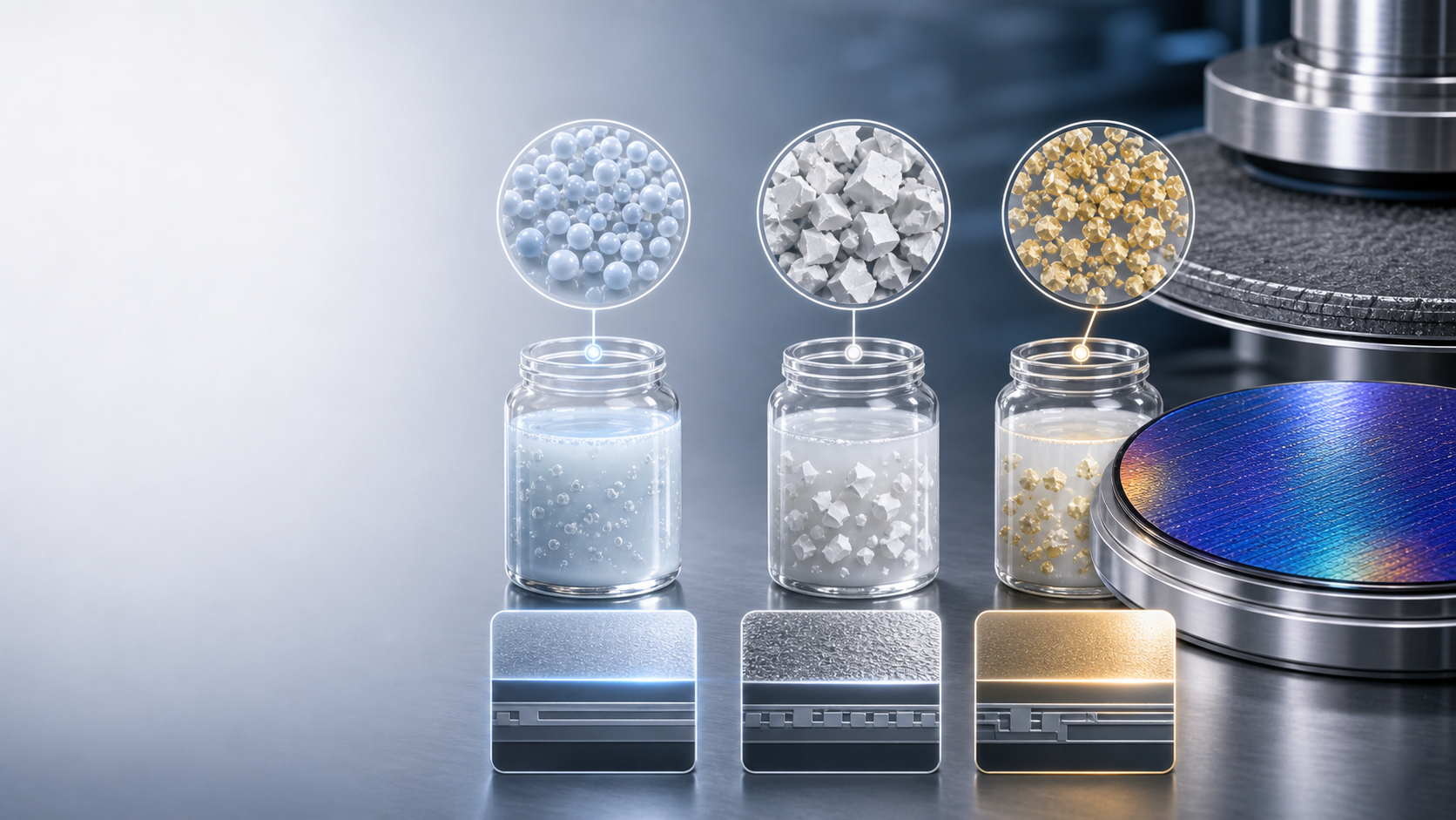
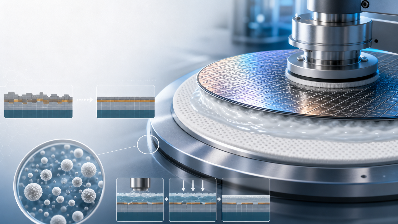
logo

Acerca de semiconductor

Este autor aún no ha rellenado ningún dato.
Hasta ahora semiconductor ha creado 185 entradas de blog.

Hard vs. Soft CMP Polishing Pads: The Definitive Selection Guide

Back to CMP Polishing Pads: The Complete Guide Jizhi Electronic Technology — Selection Guide Series A rigorous, application-mapped guide to choosing between hard and soft CMP polishing pads — covering ...

Por |2026-04-07T16:33:42+08:002026年4月7日|Blog, Industria|Comentarios desactivados en Hard vs. Soft CMP Polishing Pads: The Definitive Selection Guide

CMP Pad Materials: Polyurethane vs. All Other Options — A Complete Comparison

Back to CMP Polishing Pads: The Complete Guide Jizhi Electronic Technology — Materials Series An in-depth, property-by-property comparison of every major CMP polishing pad material — polyurethane foam, soft felt ...

Por |2026-04-07T16:32:15+08:002026年4月7日|Blog, Industria|Comentarios desactivados en CMP Pad Materials: Polyurethane vs. All Other Options — A Complete Comparison

How CMP Polishing Pads Work: Mechanisms, Physics, and Process Science

Back to CMP Polishing Pads: The Complete Guide Jizhi Electronic Technology — Fundamentals Series A rigorous, engineer-level explanation of the mechanical, chemical, and tribological mechanisms that govern material removal in ...

Por |2026-04-07T16:28:43+08:002026年4月7日|Blog, Industria|Comentarios desactivados en How CMP Polishing Pads Work: Mechanisms, Physics, and Process Science

What Is a CMP Polishing Pad? The Ultimate Guide

Back to CMP Polishing Pads: The Complete Guide Jizhi Electronic Technology — Fundamentals Series A clear, technically grounded explanation of CMP polishing pads — what they are, what they are ...

Por |2026-04-07T16:27:40+08:002026年4月7日|Blog, Industria|Comentarios desactivados en What Is a CMP Polishing Pad? The Ultimate Guide

CMP Polishing Pads: The Complete Guide for Semiconductor Professionals

Jizhi Electronic Technology — Semiconductor Materials Everything you need to know about chemical mechanical planarization pads — from material science and groove design to SiC applications, defect control, and selecting ...

Por |2026-04-07T16:27:34+08:002026年4月7日|Blog, Industria|Comentarios desactivados en CMP Polishing Pads: The Complete Guide for Semiconductor Professionals

Variación de la anchura de la ranura en el corte de obleas Causas fundamentales y métodos de control

← Back to: Diamond Dicing Blades: The Complete Guide Kerf width — the width of material removed by the dicing blade — is one of the most important dimensional output ...

Por |2026-03-16T09:44:31+08:002026年3月16日|Blog, Industria|Comentarios desactivados en Kerf Width Variation in Wafer Dicing Root Causes and Control Methods

Carga de la cuchilla para cubitos Qué es y cómo solucionarlo

← Back to: Diamond Dicing Blades: The Complete Guide Blade loading is one of the most misdiagnosed failure modes in wafer dicing. Because its symptoms — rising chipping, increasing spindle ...

Por |2026-03-16T09:44:27+08:002026年3月16日|Blog, Industria|Comentarios desactivados en Dicing Blade Loading What It Is and How to Fix It

La cuchilla se desgasta demasiado rápido: esto es lo que hay que comprobar

← Back to: Diamond Dicing Blades: The Complete Guide When a dicing blade wears out in half the expected service life, the instinct is often to blame the blade supplier. ...

Por |2026-03-16T09:44:20+08:002026年3月16日|Blog, Industria|Comentarios desactivados en Dicing Blade Wear Too Fast Heres What to Check

Dicing Blade Chipping Causes Diagnosis and Solutions

← Back to: Diamond Dicing Blades: The Complete Guide Chipping is the most common and yield-impacting defect in wafer dicing. A chip that appears to be within the die edge ...

Por |2026-03-16T09:44:16+08:002026年3月16日|Blog, Industria|Comentarios desactivados en Dicing Blade Chipping Causes Diagnosis and Solutions

QFN Package Dicing Blade Selection and Process Parameters

← Back to: Diamond Dicing Blades: The Complete Guide QFN (Quad Flat No-Lead) package singulation presents a set of dicing challenges that are qualitatively different from wafer dicing. Instead of ...

Por |2026-03-16T09:44:11+08:002026年3月16日|Blog, Industria|Comentarios desactivados en QFN Package Dicing Blade Selection and Process Parameters
Ir arriba