Top CMP Slurry Manufacturers: Global Supplier Guide
An authoritative, engineer-written reference to the world’s leading chemical mechanical planarization (CMP) slurry manufacturers — covering product portfolios, technology strengths, market share, and how to select the right partner for your fab.
Chemical mechanical planarization (CMP) is one of the most process-critical steps in semiconductor fabrication. Without a precisely engineered slurry, even the most advanced lithography and deposition tools cannot deliver the flat, defect-free surfaces required for today’s multi-layer devices. Yet selecting the right CMP slurry — and the right manufacturer to supply it — remains a challenge that spans chemistry, material science, process engineering, and global supply chain management.
This guide is designed to serve two audiences simultaneously: process engineers who need to understand formulation differences, removal rates, and selectivity trade-offs, and procurement and operations leaders who need to evaluate manufacturers by reliability, customization capability, and total cost of ownership. We have consolidated publicly available data, technical literature, and our own manufacturing expertise at JEEZ (Jizhi Electronic Technology Co., Ltd.) to give you the most comprehensive picture possible.
If you are entirely new to CMP chemistry, our foundational article — What Is CMP Slurry? A Complete Guide to Chemical Mechanical Planarization — is the recommended starting point before reading this supplier guide.
1. What Is CMP Slurry? A Quick Overview
CMP slurry is an engineered aqueous suspension that drives the material removal process during chemical mechanical planarization. It functions as the consumable interface between the polishing pad and the wafer surface, combining two distinct removal mechanisms:
- Chemical action: Oxidizers, acids, chelating agents, and pH buffers react with the target film, softening or dissolving material at the atomic scale.
- Mechanical action: Abrasive particles — most commonly ceria (CeO₂), colloidal silica (SiO₂), or alumina (Al₂O₃) — physically abrade the chemically weakened surface.
The precise balance between these two mechanisms determines removal rate (MRR), film selectivity, planarization efficiency, and post-CMP surface quality. A slurry optimized for copper interconnect removal will look chemically nothing like one designed for silicon dioxide (oxide) planarization or silicon carbide (SiC) wafer prep.
Aperçu général : No single CMP slurry formulation serves all applications. A modern 3 nm logic fab may deploy six or more distinct slurry types across its front-end and back-end process integration — each sourced, qualified, and managed as a separate consumable. Understanding the full landscape of formulations is essential before evaluating any manufacturer’s portfolio. See our detailed breakdown in CMP Slurry Types Explained: Oxide, STI, Copper, Tungsten & Beyond.
The abrasive selection alone has profound implications. Ceria-based slurries deliver extremely high oxide removal rates and superior selectivity over nitride, making them the dominant choice for STI (Shallow Trench Isolation) and ILD (Inter-Layer Dielectric) planarization. Colloidal silica, on the other hand, produces lower surface roughness and is favored for precision finishing of silicon wafers, copper, and advanced low-k dielectrics. To explore the abrasive science in depth, see our article on CMP Slurry Abrasives: Silica vs Alumina vs Ceria.
2. Global CMP Slurry Market at a Glance (2026)
The global CMP slurry market has entered a sustained growth cycle, driven by demand for advanced logic chips, DRAM scaling, 3D NAND stack height increases, and the proliferation of wide-bandgap semiconductors for power electronics and RF applications. Here are the headline figures as of mid-2026:
The market structure is moderately consolidated: a handful of large, multinational chemical companies control the majority of high-volume logic and memory slurry supply, while specialized manufacturers — including JEEZ — serve precision applications, emerging material systems (SiC, GaN), and customers requiring deep technical collaboration and rapid customization.
For a deeper look at market dynamics, regional trends, and competitive positioning, see our dedicated article: CMP Slurry Market Overview: Size, Share & Key Players (2024–2030).
3. How CMP Slurry Fits Into the Semiconductor Manufacturing Process
To evaluate any slurry manufacturer intelligently, it helps to understand exactly where CMP sits in the broader fabrication flow and why process integration requirements are so demanding.
CMP is used repeatedly throughout device fabrication — not just once. A leading-edge logic device may undergo 20 or more discrete CMP steps across its full build flow. Each step targets a different film stack, requires a different slurry chemistry, and must achieve tightly controlled thickness targets without introducing defects that propagate into subsequent layers.
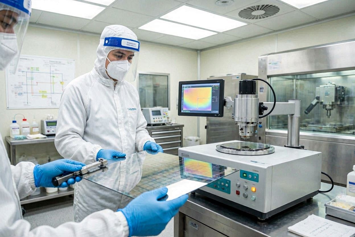
This means that a slurry supplier is not merely selling a chemical commodity. They are providing a process-integrated consumable whose performance directly determines wafer yield, throughput, and device reliability. Slurry qualification in a high-volume manufacturing environment typically requires months of characterization, process of record (POR) documentation, and ongoing statistical process control (SPC) monitoring. Switching suppliers mid-production is a significant engineering effort — making the initial supplier selection decision extremely consequential.
Engineering note: Post-CMP surface defects — including micro-scratches, large particle contamination (LPC), and residual metal ions — can have yield impacts that are orders of magnitude larger than the cost of the slurry itself. This is why evaluating manufacturers purely on price per liter is a false economy. For defect analysis methodology, see our article on Post-CMP Defect Analysis: Scratches, LPC & Inspection Methods.
4. Types of CMP Slurry: Matching Chemistry to Application
Understanding the taxonomy of CMP slurry types is the foundation for any manufacturer evaluation. A supplier who offers a broad, well-characterized portfolio across all major application categories is inherently more strategic than one with a narrow offering — even if the narrow offering excels in one area.
Each of these categories demands entirely different formulation strategies, abrasive particle selection, pH control, and additive packages. The selection process is further complicated by the fact that slurry performance is not universal — it is strongly influenced by the specific pad, tool, downforce, platen speed, and slurry flow rate used in a given fab’s process of record. For a complete treatment of each slurry type and the process parameters that govern performance, see: CMP Slurry Types Explained: Oxide, STI, Copper, Tungsten & Beyond.
5. Top CMP Slurry Manufacturers: Company-by-Company Breakdown
Below is an objective overview of the world’s most significant CMP slurry manufacturers, presented in the context of their product focus, geographic presence, and technology positioning. This is not a ranked list — each company excels in different application domains and customer segments. We include JEEZ in this section as a transparent disclosure of our own positioning.
Entegris leads the global CMP slurry market with an estimated 23% market share, following its acquisition of CMC Materials. The combined entity offers one of the broadest slurry portfolios in the industry, spanning oxide, STI, tungsten, copper, barrier, and advanced node applications. Entegris is particularly strong in logic and DRAM advanced node consumables, where its engineering teams collaborate deeply with leading foundries on next-generation integration schemes.
DuPont’s semiconductor materials division, now operating under the Qnity brand following a restructuring, is the exclusive manufacturer of the well-regarded Klebosol® silica slurry platform, as well as the Novaplane™ (tungsten), Optiplane™ (dielectric), and Acuplane™ (copper/TSV) product lines. DuPont’s slurry chemistry heritage is among the deepest in the industry, with formulations trusted across mature and advanced device nodes.
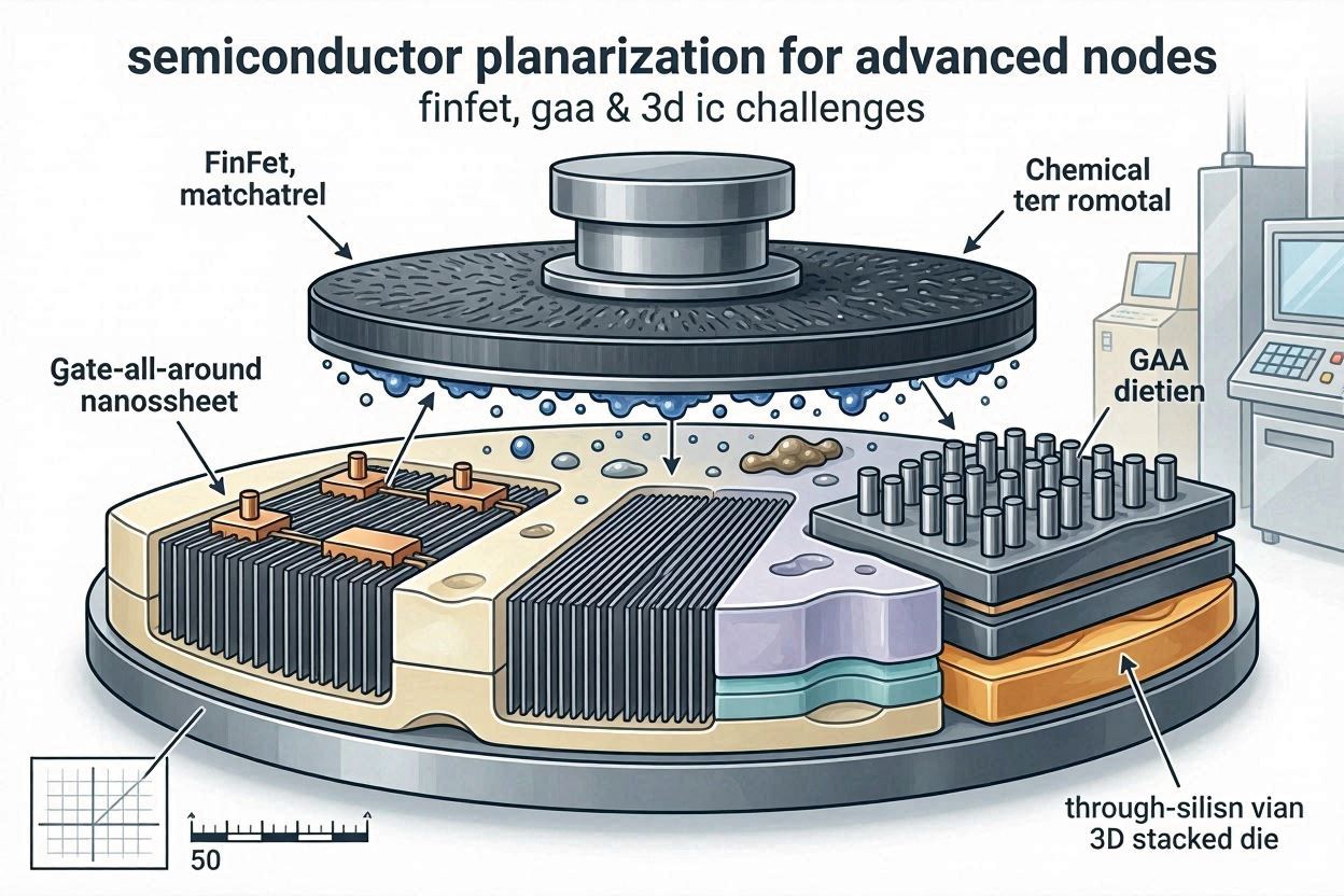
FUJIFILM Electronic Materials has built a comprehensive CMP slurry portfolio spanning copper, barrier, cobalt, front-end dielectric, and post-CMP cleaning applications. The company has invested heavily in supporting customers at advanced technology nodes (sub-7 nm), with slurries qualified for FinFET and gate-all-around (GAA) transistor processes. FUJIFILM’s strength lies in its combination of precision chemistry development and high-volume manufacturing discipline.
Resonac, formed from the merger of Showa Denko and Hitachi Chemical, supplies high-performance CMP slurries designed for semiconductor front-end processes. The company’s formulations emphasize high removal rate, excellent planarity, low defect density, and superior film selectivity — properties critical for manufacturing state-of-the-art logic and memory devices. Resonac’s integrated materials platform also covers CMP pads and other polishing consumables.
Fujimi is one of the oldest and most respected names in precision abrasive science. The company’s CMP slurries are particularly well regarded for silicon wafer final polishing and specialty abrasive applications. Fujimi’s particle engineering capabilities — controlling size distribution, morphology, and surface chemistry at the nanometer scale — give its slurries exceptional consistency and low defectivity, which is critical for bare silicon and epitaxial wafer preparation.
AGC differentiates itself as a fully integrated CMP slurry manufacturer — producing its own abrasive particles in-house before incorporating them into finished slurry formulations. This vertical integration from abrasive production to finished slurry gives AGC tight control over particle quality and supply chain security. AGC’s portfolio covers silicon-based films (poly-Si, SiO₂, SiN), metals, and resins across front-end, back-end, packaging, and specialty semiconductor applications.
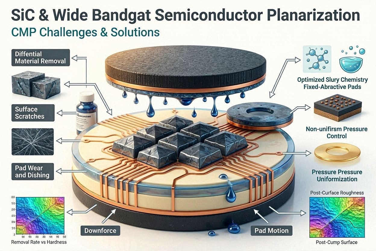
Saint-Gobain brings centuries of advanced materials expertise to the CMP slurry market. Its alumina polishing slurries are particularly recognized for delivering enhanced removal rates and superior planarization performance on silicon carbide wafers, making Saint-Gobain a go-to supplier for the rapidly expanding SiC power device market. The company also offers oxide and copper CMP slurries with strong surface finish characteristics.
Cabot Microelectronics — now operating as part of Cabot Corporation — was for many years the world’s single largest CMP slurry supplier by volume. The company’s legacy in the copper CMP market is particularly deep, with slurry platforms that have been qualified at essentially every leading-edge foundry globally. Cabot’s scale and global manufacturing footprint make it a reliable choice for high-volume commodity applications, though its pricing structure reflects its market position.
South Korea has emerged as a significant force in CMP slurry supply, anchored by domestic demand from Samsung and SK Hynix. KCTech and Soulbrain have both built credible portfolios of oxide, STI, and copper slurries with increasingly competitive technical performance. Samsung SDI contributes materials science capabilities from its broader battery and materials business. These suppliers benefit from geographic proximity to the world’s largest memory manufacturers.
6. JEEZ: A Precision-Focused CMP Slurry Manufacturer
JEEZ — Jizhi Electronic Technology Co., Ltd.
Headquartered in China · Manufacturing & R&D integrated · ISO-certified production
JEEZ designs and manufactures CMP slurries with a focus on precision applications, emerging wide-bandgap semiconductor materials, and customers who require deep technical collaboration rather than off-the-shelf commodity supply. Our in-house R&D team works directly with process engineers to develop application-specific formulations, and our manufacturing processes are designed for the particle size consistency and metallic impurity levels that advanced device nodes demand.
JEEZ’s approach to CMP slurry manufacturing is built on three principles: formulation precision (tightly controlled abrasive particle size distribution and zeta potential), process integration support (our application engineers work on-site with customers during qualification), and supply chain reliability (dedicated production capacity and dual raw material sourcing).
Why Customers Choose JEEZ for CMP Slurry
While global giants compete primarily on volume and legacy node dominance, JEEZ has built its competitive position around four differentiating factors:
- Wide-bandgap semiconductor expertise: SiC and GaN polishing presents abrasive challenges that many conventional slurry portfolios are not optimized to address. JEEZ has dedicated formulation programs for SiC wafer preparation, including both the substrate polishing and epi-ready finishing stages. Learn more about the specific challenges and our approach in CMP Slurry for SiC Wafer Polishing: Challenges & Solutions.
- Rapid customization cycle: For customers with non-standard film stacks, unusual selectivity requirements, or process integration constraints not served by catalog products, JEEZ’s R&D team can develop and iterate on custom formulations significantly faster than large multi-national suppliers, whose product development pipelines are necessarily longer and more rigid.
- Application engineering partnership: JEEZ assigns dedicated application engineers to key accounts. These engineers understand both the slurry chemistry and the CMP tool mechanics — enabling them to help customers optimize pad conditioning, slurry flow rate, and process parameters alongside the slurry formulation itself.
- Transparent cost structure: JEEZ provides detailed cost-of-ownership (CoO) analyses for customers evaluating slurry transitions. This includes removal rate per wafer, dilution ratio impact, post-CMP defect reduction value, and yield improvement modeling — not just a price-per-liter comparison.
Advanced packaging note: As chipmakers migrate to 2.5D and 3D integration architectures, CMP requirements for through-silicon via (TSV) reveal, redistribution layer (RDL) planarization, and hybrid bonding surface preparation are evolving rapidly. JEEZ is actively developing slurry solutions for these emerging applications. See our dedicated overview: Advanced Packaging CMP: Slurry Requirements for 3D NAND & TSV Processes.
7. Manufacturer Comparison at a Glance
The table below provides a high-level comparison of key manufacturers across application coverage, geographic presence, and key strengths. This is intended as an orientation tool, not a definitive capability assessment — slurry performance is highly process-specific and must be evaluated through direct qualification.
For a deeper head-to-head analysis of the four largest players, see: CMP Slurry Manufacturers Comparison: Cabot vs DuPont vs Fujifilm vs Entegris.
| Manufacturer | QG | Oxide/STI | Cu / W | SiC / WBG | Adv. Packaging | Custom Formulation | Key Strength |
|---|---|---|---|---|---|---|---|
| Entegris | ÉTATS-UNIS | ✔ | ✔ | ◑ | ✔ | ◑ | Largest portfolio, advanced node logic/DRAM |
| DuPont / Qnity | ÉTATS-UNIS | ✔ | ✔ | ◑ | ✔ | ◑ | Klebosol® legacy; deep tungsten expertise |
| FUJIFILM EM | Japon | ✔ | ✔ | ◑ | ✔ | ◑ | Cobalt/Ru; sub-7nm node readiness |
| Resonac | Japon | ✔ | ✔ | ◑ | ◑ | ◑ | Low defect, high planar uniformity |
| Fujimi | Japon | ✔ | ◑ | ◑ | ✗ | ◑ | Si wafer polishing; particle precision |
| AGC | Japon | ✔ | ✔ | ◑ | ✔ | ✔ | Vertically integrated; abrasive-to-slurry |
| Saint-Gobain | France | ✔ | ◑ | ✔ | ◑ | ◑ | SiC/sapphire; advanced alumina |
| KCTech / Soulbrain | Korea | ✔ | ✔ | ✗ | ◑ | ◑ | Memory fab proximity; competitive pricing |
| JEEZ | China | ✔ | ✔ | ✔ | ✔ | ✔ | SiC/WBG expertise; rapid customization; engineering partnership |
✔ Full coverage | ◑ Partial / limited portfolio | ✗ Not a primary focus. This table reflects publicly available product information as of May 2026 and is subject to change as manufacturers expand their portfolios.
8. How to Choose a CMP Slurry Manufacturer
Choosing a CMP slurry manufacturer is a strategic decision that goes well beyond product specifications. The following framework is designed to help both engineering teams and procurement organizations structure their evaluation process systematically.
Step 1: Define Your Application Requirements
Start with the target film system (oxide, metal, dielectric, WBG), the technology node or device generation, and the specific performance targets — removal rate range, within-wafer uniformity (WiWNU), selectivity requirements, and maximum allowable defect density. Many fabs underspecify at this stage and end up qualifying slurries that technically meet stated specs but fail to deliver the margin needed for high-volume manufacturing.
Step 2: Evaluate Portfolio Breadth vs. Specialization
A supplier with a broad portfolio can streamline your supply base — fewer vendor qualifications, consolidated logistics, simpler quality management. However, specialized manufacturers often offer deeper expertise in specific application domains and greater flexibility for customization. The right choice depends on whether your process is predominantly mainstream (logic FEOL, copper BEOL) or involves emerging materials, unusual selectivity requirements, or non-standard integration schemes.
Caution: Avoid selecting a slurry supplier based solely on name recognition or market share. A supplier’s historical excellence in copper CMP for leading-edge logic does not necessarily translate to competence in SiC wafer polishing or advanced packaging CMP — these require entirely different chemistry platforms and abrasive engineering capabilities.
Step 3: Assess Technical Support Depth
The quality of applications engineering support is often the decisive factor in difficult qualifications. Ask prospective suppliers: Do they have dedicated application engineers who can be present at your tool during process development? Do they provide formulation data (particle size distribution, zeta potential, pH stability curves) rather than just product specs? Can they share case studies from comparable integration schemes? A supplier who can answer these questions comprehensively is worth more than one with a lower line-item price.
Step 4: Qualify Supply Chain Reliability
Slurry supply interruptions translate directly to fab downtime. Evaluate: Are raw materials single-sourced? What is the supplier’s safety stock policy? Do they have production capacity redundancy? For customers in geopolitically sensitive regions, local or regional manufacturing presence may be a prioritized criterion. This is one area where JEEZ’s China-based manufacturing can offer meaningful advantages for Asia-Pacific customers.
Step 5: Calculate Total Cost of Ownership (CoO)
Per-liter slurry price is the least meaningful cost metric in CMP. A slurry with a higher removal rate may consume less volume per wafer, delivering lower cost per wafer even at a higher unit price. Similarly, a slurry that reduces post-CMP defect density can deliver yield improvement worth many multiples of the consumable cost difference. Always model CoO across the full process context, not on a per-liter basis alone.
For a structured technical approach to slurry selection from the process engineering perspective, see our dedicated guide: How to Choose a CMP Slurry: Selection Guide for Semiconductor Engineers.
9. Emerging Trends Shaping the CMP Slurry Industry
The CMP slurry market is not static. Several converging trends are reshaping what manufacturers need to offer and how procurement teams need to think about their supply strategies.
Wide-Bandgap Semiconductor Expansion
SiC-based power devices are ramping rapidly for EV drivetrains, industrial inverters, and renewable energy systems. SiC’s extreme hardness (Mohs 9.5) makes conventional silica and alumina slurries impractical for production-rate polishing — material removal rates fall below 20 nm/min, creating throughput bottlenecks. This is driving demand for diamond slurries and specialized ceria formulations capable of chemically assisted MRR enhancement on SiC surfaces. GaN-on-SiC and GaN-on-Si substrates for RF and power applications present similar challenges. Manufacturers who have invested in WBG-specific slurry platforms are well positioned for significant growth. See our full technical discussion: CMP Slurry for SiC Wafer Polishing: Challenges & Solutions.
Advanced Packaging and 3D Integration
As Moore’s Law scaling slows, the industry is turning to advanced packaging — chiplets, 2.5D interposers, 3D-stacked memory, and fan-out wafer-level packaging — as the primary path to continued performance improvement. Each of these integration approaches introduces new CMP requirements: thick copper removal for TSV reveal, ultra-flat surfaces for hybrid bonding, and RDL planarization. These applications require slurries with different selectivity profiles and defect control requirements than front-end CMP, creating new product development opportunities for manufacturers willing to invest in process integration knowledge. Our technical overview covers these requirements in detail: Advanced Packaging CMP: Slurry Requirements for 3D NAND & TSV Processes.
Abrasive-Free and Ultra-Low-Concentration Slurries
For the most sensitive applications — particularly low-k dielectric planarization and advanced barrier CMP — the semiconductor industry is exploring abrasive-free formulations and ultra-dilute slurry systems that rely predominantly on chemical action rather than mechanical abrasion. These approaches aim to minimize scratch defects and subsurface damage in mechanically fragile materials, though they require very precise process control and often demand longer polish times. This is an active area of research that is likely to influence the next generation of BEOL CMP consumables.
Cobalt and Ruthenium Interconnects
As copper scaling encounters resistivity and electromigration limits at advanced nodes (below 7 nm), cobalt (Co) and ruthenium (Ru) are being introduced as liner materials, cap layers, and in some cases primary conductors. Each of these materials requires dedicated CMP chemistry — neither behaves like copper or tungsten under existing slurry formulations. The development of Co and Ru slurries has been an active priority at leading manufacturers since approximately 2020, and commercial formulations are now available for production use at select nodes.
Sustainability and Chemical Waste Reduction
CMP is a significant consumer of deionized water and generates slurry waste that must be managed carefully. Environmental regulations and corporate sustainability targets are driving interest in slurry recycling and reclaim systems, as well as concentrated slurry formulations that reduce shipping volume and on-site dilution waste. Manufacturers who can offer slurries with reduced environmental footprint — both in production and in use — are increasingly advantaged in customer evaluations, particularly in jurisdictions with stringent industrial wastewater regulations.
10. Frequently Asked Questions
Ready to Discuss Your CMP Slurry Requirements?
Whether you are qualifying a new process, evaluating a supplier transition, or developing a slurry solution for an emerging material system — JEEZ’s application engineering team is ready to work with you. We offer no-obligation technical consultations, process window data from prior deployments, and rapid prototype formulation programs for non-standard applications.
Contact Our Experts →