CMP Equipment for Advanced Node Manufacturing
Table des matières
- Why Advanced Nodes Change CMP Requirements
- CMP Challenges at Leading-Edge Nodes
- TSV Reveal for 3D Integration
- Redistribution Layer (RDL) Polishing
- Hybrid Bonding Surface Preparation
- 3D NAND and HBM Stacking Considerations
- Equipment Requirements for Advanced Manufacturing
- Consumable Considerations
- Questions fréquemment posées
Why Advanced Nodes Change CMP Requirements
At older process nodes, CMP equipment requirements were comparatively modest: planarize a handful of dielectric and metal layers within tolerances that, while demanding, left some margin for variation. As nodes have moved to 7nm and below, and as advanced packaging has added entirely new categories of CMP steps, the margin for variation has shrunk dramatically while the number of CMP steps per wafer has grown.
This combination — more steps, tighter tolerances, and a wider variety of materials being polished — means that CMP equipment for advanced manufacturing needs to deliver not just better average performance, but more consistent performance across every wafer, every lot, and every tool in a fleet.
CMP Challenges at Leading-Edge Nodes
At leading-edge logic nodes, several factors combine to make CMP more demanding than in previous generations. Interconnect stacks now include many more metal layers, each requiring its own CMP step with tight within-wafer non-uniformity (WIWNU) targets to avoid yield-limiting variation across the die.
Low-k and ultra-low-k interlayer dielectrics, introduced to reduce capacitance between interconnects, are mechanically more fragile than traditional oxide films and are more susceptible to damage during polishing if pressure, pad selection, and slurry chemistry are not carefully matched to the film stack. Copper damascene structures at advanced nodes also have finer line widths and tighter pitch, which increases sensitivity to dishing and erosion — topics we cover in more depth in How CMP Equipment Works.
Taken together, these factors mean that CMP equipment serving leading-edge logic fabs needs tighter process control, more sophisticated endpoint detection, and often more frequent consumable changeovers than equipment running older nodes.
TSV Reveal for 3D Integration
Through-silicon vias (TSVs) are a core enabling technology for 3D chip integration, allowing electrical connections to pass vertically through a silicon die. After TSVs are formed and the wafer is thinned, a CMP step — often called TSV reveal — is used to expose the via structures at the wafer surface with a controlled, planar profile.
TSV reveal CMP differs from front-end CMP in several ways: it typically operates on thinned wafers that are more fragile and prone to warpage, and it must achieve planarity across via structures and surrounding silicon or dielectric without causing via protrusion or recess that would affect subsequent bonding or interconnect steps. Equipment used for TSV reveal often requires specialized wafer handling to accommodate thinned-wafer fragility alongside the polishing module itself.
Redistribution Layer (RDL) Polishing
Redistribution layers (RDL) are used in advanced packaging to fan out connections from a die’s native pad pitch to a wider pitch suitable for package-level interconnects. RDL structures typically involve polymer dielectrics and copper or aluminum routing layers, which require CMP steps with different material removal characteristics than front-end interconnect CMP.
Because RDL layers are often built on reconstituted wafers or panels that may include multiple dies with slightly different topographies, CMP equipment used for RDL polishing needs to accommodate a wider range of starting topography while still achieving the planarity needed for subsequent lithography and via formation steps.
Hybrid Bonding Surface Preparation
Hybrid bonding — which joins two wafers or dies through a combination of dielectric and direct copper-to-copper bonding without traditional solder bumps — places some of the most stringent surface requirements of any CMP application. Successful hybrid bonding requires extremely flat, clean, and chemically prepared surfaces on both bonding partners, since even nanometer-scale topography variations or surface contamination can result in voids or weak bonds.
3D NAND and HBM Stacking Considerations
3D NAND flash memory and high-bandwidth memory (HBM) both rely on stacking many layers — either as deposited film stacks within a single die or as multiple stacked dies connected through TSVs and hybrid bonding. In 3D NAND, CMP is used repeatedly across the deposition and etch cycles that build up the layer stack, with each CMP step needing to maintain planarity across an increasingly tall and complex structure.
For HBM, CMP plays a role both in building the individual memory dies and in preparing surfaces for the TSV and bonding steps that stack those dies together. As HBM stack heights increase generation over generation, the cumulative impact of any CMP-related variation across the stack becomes more significant, reinforcing the importance of consistent, well-controlled CMP performance at every step.
Equipment Requirements for Advanced Manufacturing
Tighter Process Control
Advanced node and advanced packaging CMP steps demand tighter WIWNU and removal rate control, often requiring more sophisticated platen and carrier head designs.
In-Situ Endpoint Detection
Real-time monitoring becomes more important as process windows narrow, helping equipment stop polishing at precisely the right point across a wider variety of film stacks.
Thinned-Wafer Handling
TSV reveal and other advanced packaging steps often involve thinned or reconstituted wafers, requiring handling systems designed to avoid breakage or warpage-related defects.
Integrated Cleaning
Surface cleanliness requirements for hybrid bonding and other advanced steps place additional demands on integrated cleaning modules — see CMP Equipment Cleaning and Contamination Control.
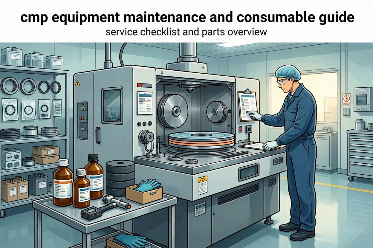
Consumable Considerations
The shift toward advanced node and advanced packaging CMP also changes consumable requirements. New film stacks and materials — low-k dielectrics, polymer RDL layers, exposed TSV structures — often require pad and slurry combinations distinct from those used in conventional front-end CMP, and qualification cycles for these consumables need to account for the tighter tolerances involved.
As we discuss in CMP Equipment Market Trends 2026, the growth in advanced packaging adoption is a significant driver of overall CMP consumable demand, since each additional CMP step in a process flow represents additional pad, slurry, and conditioner consumption. For fabs running a mix of 300mm front-end and advanced packaging process flows, the wafer-size and equipment differences covered in 300mm vs 200mm CMP Equipment Differences can also factor into consumable sourcing decisions.
For a broader view of how these process steps fit into overall CMP equipment architecture, return to our complete CMP equipment guide.
Need Consumables Qualified for Advanced Node or Advanced Packaging CMP?
JEEZ works with fabs to qualify polishing pads, slurries, and conditioners for demanding advanced process flows. Get in touch with our technical team.
Nous contacterQuestions fréquemment posées
What is TSV reveal CMP used for?
TSV reveal is a CMP step that exposes through-silicon via structures at the surface of a thinned wafer with a controlled, planar profile, enabling subsequent bonding or interconnect steps in 3D chip integration.
Why does hybrid bonding require special CMP and cleaning steps?
Hybrid bonding requires extremely flat, clean, and chemically prepared surfaces on both bonding partners, since nanometer-scale topography variations or contamination can cause voids or weak bonds, driving requirements for highly controlled CMP and cleaning sequences.
How does 3D NAND manufacturing use CMP differently than logic manufacturing?
3D NAND relies on repeated CMP steps across deposition and etch cycles to maintain planarity across an increasingly tall layer stack, whereas logic manufacturing primarily uses CMP to planarize interconnect layers at each metal level.
Why do advanced node and advanced packaging processes require different CMP consumables?
New film stacks such as low-k dielectrics, polymer RDL layers, and exposed TSV structures often require pad and slurry combinations distinct from conventional front-end CMP, with qualification cycles that account for tighter process tolerances.