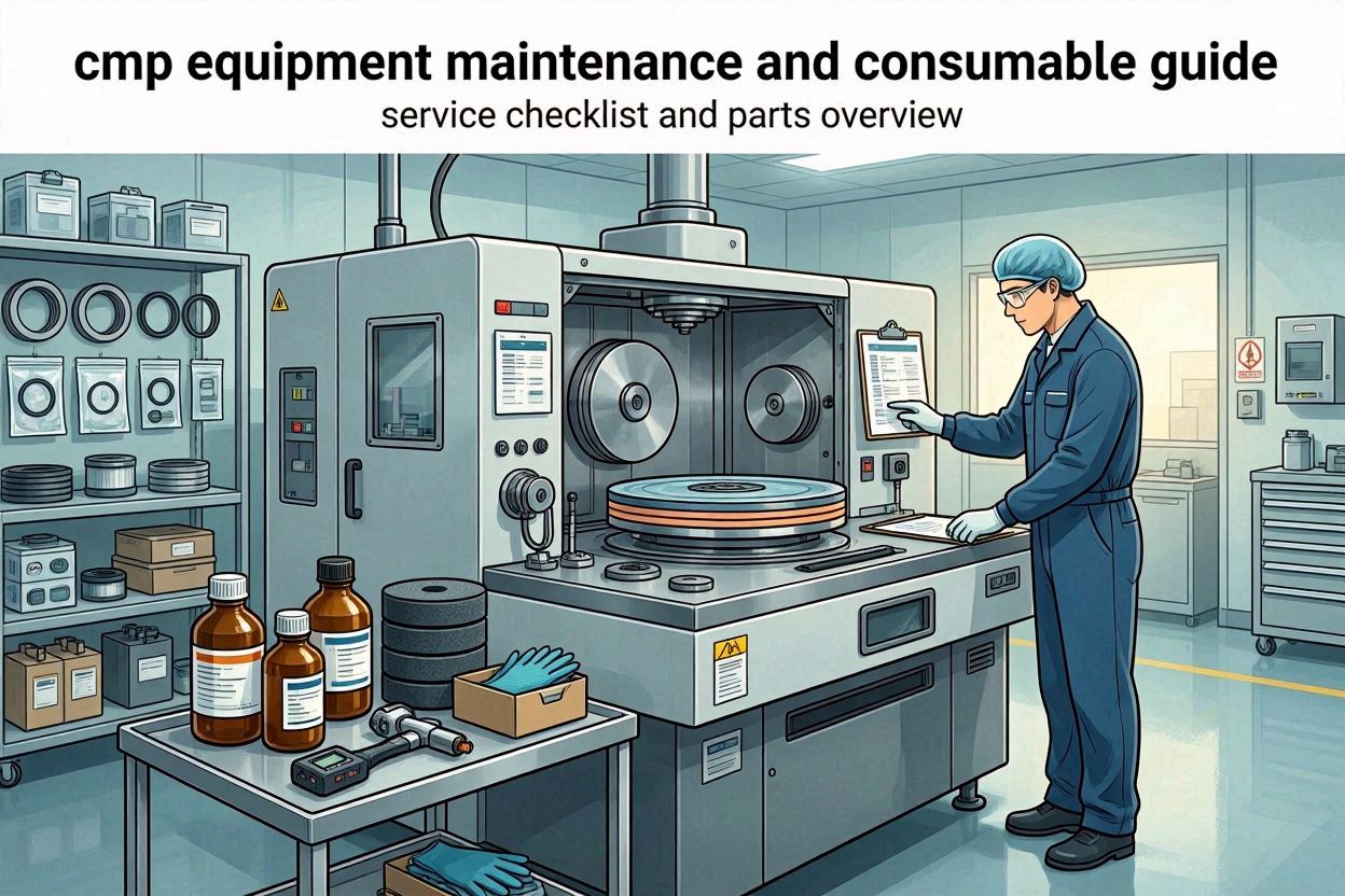
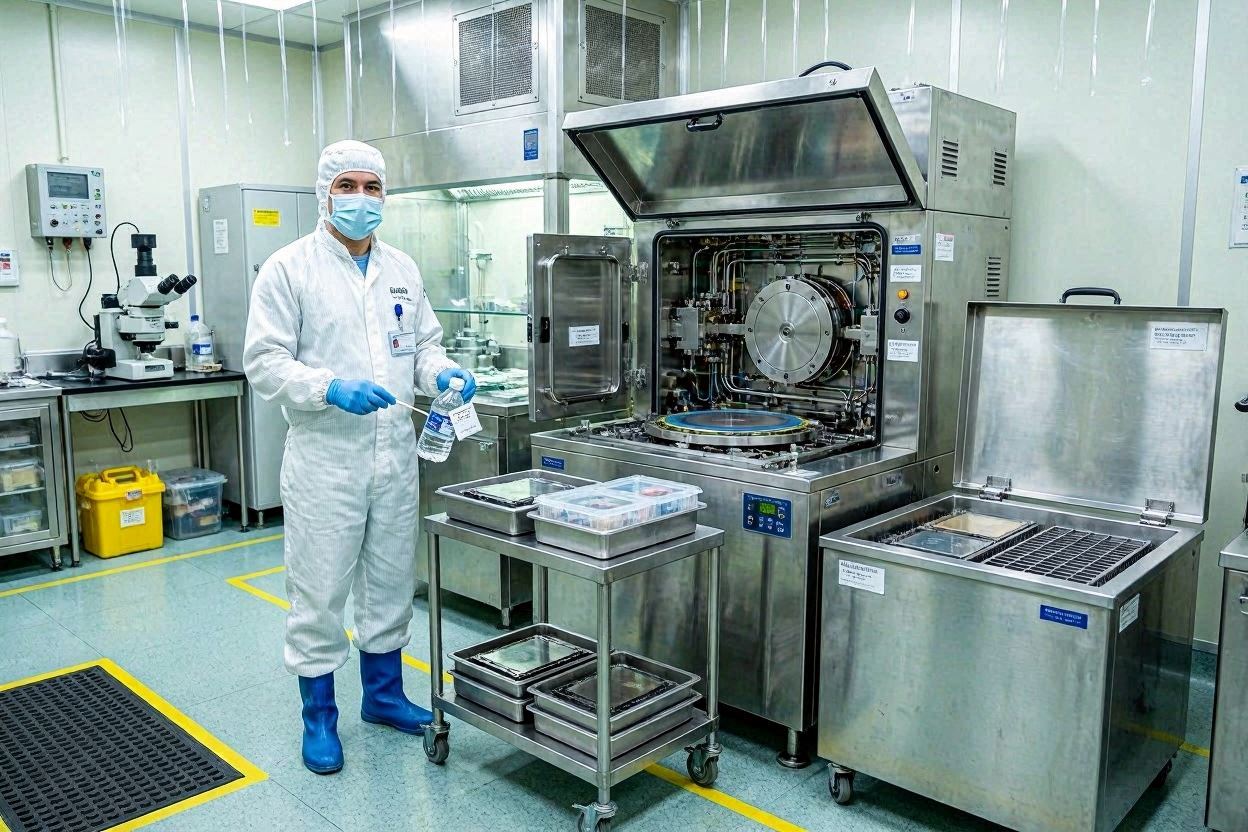
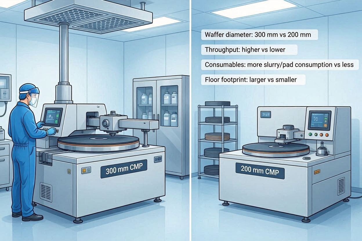
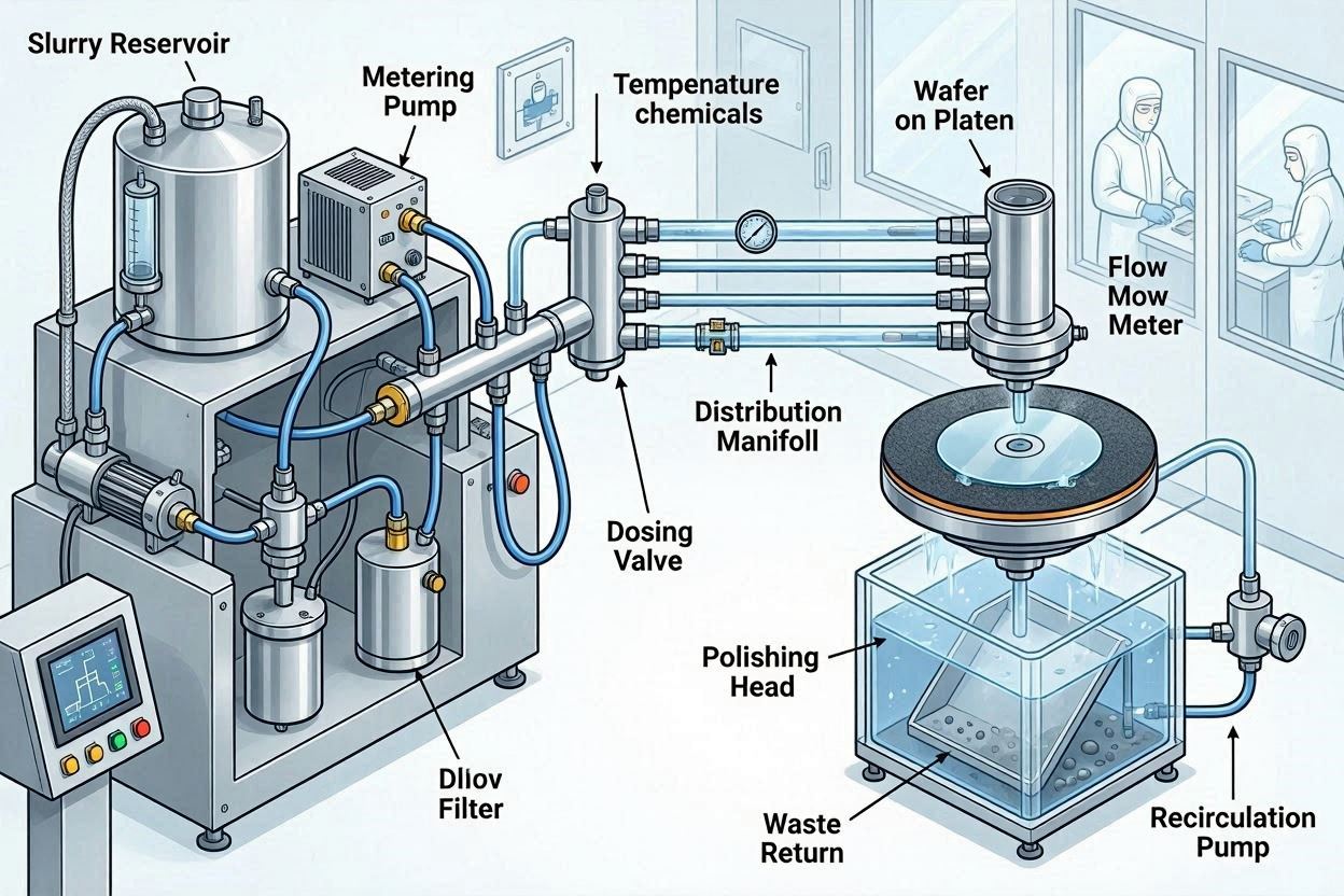
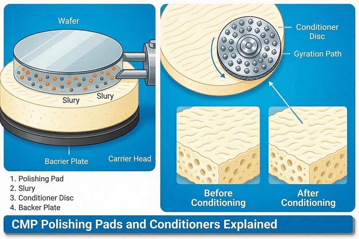
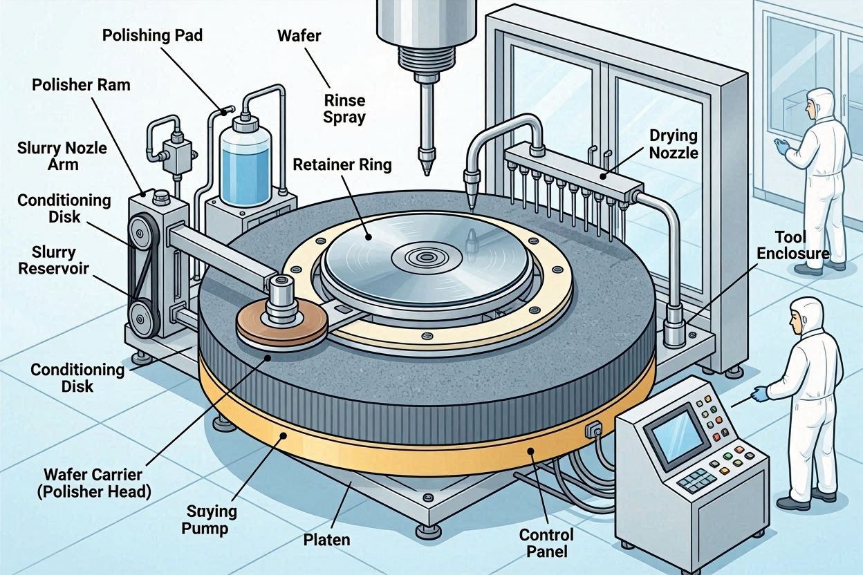
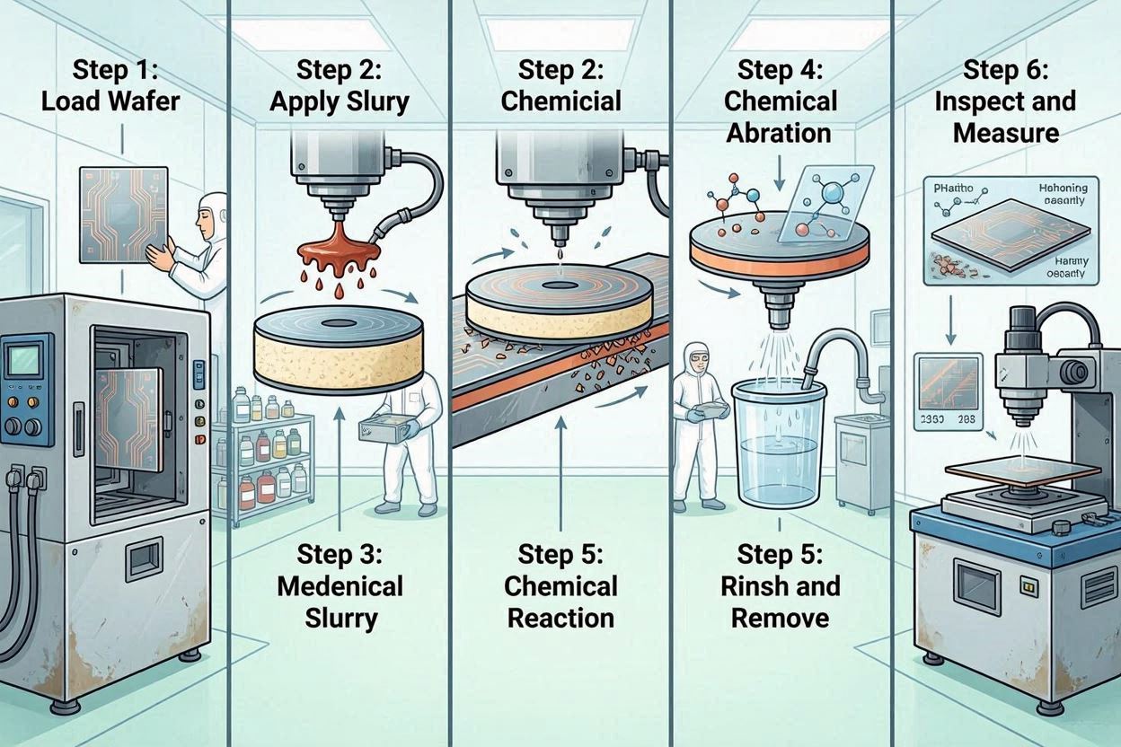
logo

À propos de semiconductor

Cet auteur n'a pas encore fourni de détails.
Jusqu'à présent, semiconductor a créé 185 entrées de blog.

CMP in Advanced Nodes:Challenges at 7nm, 5nm & Beyond

Advanced Technology · Updated May 2026 A detailed technical analysis of how CMP requirements evolve at leading-edge logic nodes — covering new device architectures (GAA, CFET), new interconnect materials (cobalt, ...

Par |2026-05-19T14:16:31+08:002026年5月19日|Blog, L'industrie|Commentaires fermés sur CMP in Advanced Nodes:Challenges at 7nm, 5nm & Beyond

CMP Polishing Pad:Types, Selection & Performance Guide

Materials Engineering · Updated May 2026 Everything process engineers need to know about CMP polishing pads — covering material types, hardness trade-offs, groove geometry, pad conditioning, multi-stack configurations, lifetime management, ...

Par |2026-05-19T14:15:54+08:002026年5月19日|Blog, L'industrie|Commentaires fermés sur CMP Polishing Pad:Types, Selection & Performance Guide

Post-CMP Cleaning:Methods, Challenges & Best Practices

Process Engineering · Updated May 2026 A complete technical guide to post-CMP wafer cleaning — covering contamination types, brush scrub and megasonic methods, cleaning chemistry selection, metallic contamination control, advanced-node ...

Par |2026-05-19T14:15:18+08:002026年5月19日|Blog, L'industrie|Commentaires fermés sur Post-CMP Cleaning:Methods, Challenges & Best Practices

CMP Slurry Guide:Types, Selection & Optimization

Materials Engineering · Updated May 2026 A comprehensive technical reference for process engineers and procurement specialists — covering abrasive chemistry, slurry formulation, application-specific selection criteria, stability requirements, and optimization strategies ...

Par |2026-05-19T14:14:01+08:002026年5月19日|Blog, L'industrie|Commentaires fermés sur CMP Slurry Guide:Types, Selection & Optimization

CMP Process Step-by-Step:How Wafer Polishing Works

Process Engineering · Updated May 2026 A complete engineering walkthrough of every stage in the Chemical Mechanical Planarization process — from wafer loading and slurry delivery to endpoint detection and ...

Par |2026-05-19T14:12:50+08:002026年5月19日|Blog, L'industrie|Commentaires fermés sur CMP Process Step-by-Step:How Wafer Polishing Works

CMP Semiconductor:The Complete Guide to Chemical Mechanical Planarization

Complete Technical Guide · Updated May 2026 Everything engineers, procurement specialists, and researchers need to know about Chemical Mechanical Planarization — from first principles to advanced-node challenges, consumable selection, defect ...

Par |2026-05-19T14:23:10+08:002026年5月19日|Blog, L'industrie|Commentaires fermés sur CMP Semiconductor:The Complete Guide to Chemical Mechanical Planarization

Advanced Packaging CMP: Slurry Requirements for 3D NAND & TSV Processes

Advanced Technology Guide · Updated May 2026 A technical deep dive into CMP slurry requirements for advanced semiconductor packaging — covering through-silicon via reveal, redistribution layer planarization, hybrid bonding surface ...

Par |2026-05-13T11:22:50+08:002026年5月13日|Blog, L'industrie|Commentaires fermés sur Advanced Packaging CMP: Slurry Requirements for 3D NAND & TSV Processes

Post-CMP Defect Analysis: Scratches, LPC & Inspection Methods

Process Engineering Guide · Updated May 2026 A practical guide to understanding, characterizing, and eliminating the most common post-CMP defect types — covering scratch morphology, large particle contamination, inspection equipment ...

Par |2026-05-13T11:22:03+08:002026年5月13日|Blog, L'industrie|Commentaires fermés sur Post-CMP Defect Analysis: Scratches, LPC & Inspection Methods

CMP Slurry for SiC Wafer Polishing: Challenges & Solutions

Vertical Application Guide · Updated May 2026 A comprehensive technical guide to CMP slurry selection and process development for silicon carbide substrate polishing — covering the unique challenges of SiC's ...

Par |2026-05-13T11:17:58+08:002026年5月13日|Blog, L'industrie|Commentaires fermés sur CMP Slurry for SiC Wafer Polishing: Challenges & Solutions

CMP Slurry Abrasives Explained: Silica vs Alumina vs Ceria

Technical Deep Dive · Updated May 2026 A detailed technical comparison of the three dominant abrasive types used in semiconductor CMP slurries — covering particle chemistry, hardness, size effects, removal ...

Par |2026-05-13T11:15:05+08:002026年5月13日|Blog, L'industrie|Commentaires fermés sur CMP Slurry Abrasives Explained: Silica vs Alumina vs Ceria
Haut de page