CMP Pad Materials: Polyurethane vs. All Other Options — A Complete Comparison
An in-depth, property-by-property comparison of every major CMP polishing pad material — polyurethane foam, soft felt composites, fixed-abrasive pads, poreless polymer films, and next-generation alternatives — with guidance on matching material to application.
Verified
- Why Pad Material Is the Foundation
- Polyurethane (Filled / Porous) — The Industry Standard
- Soft Polyurethane Foam — Cu BEOL Specialist
- Non-Woven Fiber Composites — Legacy and Substrate Work
- Fixed-Abrasive Pads — High-Hardness Applications
- Poreless Polymer Films — Next-Generation Architecture
- Master Comparison: All Materials Side by Side
- Material Selection Decision Framework
- Polyurethane Chemistry Deep Dive
- FAQ
The choice of pad material is the single most consequential design decision in CMP polishing pad engineering. It determines the hardness ceiling and floor achievable by formulation, the slurry retention mechanism available, the chemical compatibility with aggressive slurry systems, and the thermal stability at process temperatures. Every other pad design variable — groove geometry, pore size distribution, backing layer — operates within the envelope set by the base material.
Yet pad material selection is poorly documented in publicly available literature. Suppliers typically describe their pads by product family name — IC1000, Politex, Trizact — rather than by material class, making cross-supplier comparisons difficult. This article provides the systematic, material-class-level analysis that fab engineers and procurement teams need. If you are new to CMP pads and want context before this deep dive, start with: What Is a CMP Polishing Pad? The Ultimate Guide.
1. Why Pad Material Is the Foundation of Everything Else
Before examining each material class, it is worth establishing precisely which properties are material-determined versus design-determined in a CMP pad. This distinction clarifies why material selection must come first in pad engineering.
🔩 Material-Determined Properties
- Bulk hardness range (Shore A/D)
- Glass transition temperature (Tg) — thermal ceiling
- Chemical resistance to slurry reagents (oxidizers, pH extremes)
- Elastic modulus and creep behavior under sustained load
- Inherent porosity type (open-cell, closed-cell, poreless)
- Surface wettability with aqueous slurries
- Maximum operating temperature before property degradation
🔧 Design-Determined Properties (Within Material Envelope)
- Precise hardness value (via formulation within material range)
- Pore size and density (via microsphere selection and loading)
- Groove geometry (machined post-curing)
- Pad thickness (set by casting process)
- Backing layer type and PSA specification
- Surface texture after conditioning (conditioner-dependent)
This framework explains why a soft polyurethane pad, no matter how expertly formulated, cannot be made as hard as a fixed-abrasive diamond pad — the material ceiling is absolute. Similarly, a non-woven fiber pad cannot be made poreless by design modification; its intrinsic fibrous structure defines its slurry retention mechanism. Understanding these constraints prevents engineers from trying to push a material beyond its inherent capability.
2. Filled Polyurethane (Porous Hard Pad) — The Industry Standard
Filled, closed-cell polyurethane foam is by far the dominant CMP pad material in high-volume semiconductor manufacturing. It is the reference material against which all alternatives are benchmarked. Understanding its structure, chemistry, and property range in depth is essential context for evaluating alternatives. For how this material functions during polishing, see: How CMP Polishing Pads Work.
Polyurethane Synthesis and the Hardness Knob
Polyurethane is synthesized by the condensation reaction of a polyfunctional isocyanate with a polyol. The ratio of isocyanate groups to hydroxyl groups (the NCO/OH index) is the primary lever controlling cross-link density and therefore hardness. A higher NCO/OH index yields a more tightly cross-linked network, a higher Young’s modulus, and a higher Shore D hardness. The polyol backbone type — polyether, polyester, or polycarbonate — governs hydrolytic stability, low-temperature flexibility, and chemical resistance.
The Role of Hollow Microspheres
The pore structure in filled PU CMP pads is created by dispersing hollow polymeric microspheres (typically expanded acrylonitrile or polyvinylidene chloride shells, 20–50 µm in diameter) into the PU precursor mixture before curing. The microspheres remain intact during curing, forming a closed-cell architecture rather than the open-cell foam of a conventional sponge. Key microsphere parameters and their process effects:
| Microsphere Parameter | Effect on Pad Properties | Effect on CMP Process |
|---|---|---|
| Mean diameter (µm) ↑ | Larger pores, lower effective bulk density, lower hardness | Higher slurry reservoir capacity; slightly lower contact area |
| Size distribution (CV%) ↑ | Wider variation in local surface texture after conditioning | Higher within-pad MRR non-uniformity; wider removal rate distribution |
| Loading (volume fraction) ↑ | Lower effective hardness; higher compressibility | Better wafer conformance; lower planarization efficiency |
| Shell wall thickness ↑ | Stiffer microspheres; higher effective bulk modulus | More consistent pore exposure after conditioning; fewer debris fragments |
3. Soft Polyurethane Foam — The Cu BEOL and Low-k Specialist
Soft polyurethane pads use a lower NCO/OH index and higher microsphere loading than hard pads, yielding a more open, compliant polymer network. The lower Young’s modulus — typically 10–60 MPa versus 200–500 MPa for hard PU — means that under applied down-force, the pad surface conforms to wafer-scale topography rather than bridging over it. This conformance delivers two benefits:
- Improved edge-center uniformity: The compliant pad accommodates wafer bow and warp (common in 300 mm wafers post-stress-inducing deposition steps), distributing contact pressure more evenly from center to edge.
- Lower shear stress on fragile films: The reduced contact stiffness lowers peak shear forces at the pad-wafer interface — critical for protecting porous low-k dielectrics (k < 2.5), which can delaminate or crack under the shear forces generated by hard pads at standard process pressures.
The trade-off is reduced planarization efficiency. A soft pad that conforms to topography cannot preferentially remove from high points — it removes everywhere. For the detailed hard-versus-soft selection framework with application mapping, see: Hard vs. Soft CMP Polishing Pads: Selection Guide.
4. Non-Woven Fiber Composites — Legacy Oxide and Substrate Applications
Non-woven fiber composite pads consist of a mat of synthetic fibers (polyester, nylon, or polyaramid) bonded by a PU impregnant that fills the inter-fiber spaces. The fibrous architecture creates a highly open, interconnected pore network with extremely high slurry uptake — the pad behaves almost like a sponge, absorbing and releasing slurry readily. This makes fiber pads forgiving of slurry flow interruptions and effective at maintaining a continuously replenished slurry film across a large contact area.
The limitations of fiber pads are significant for advanced semiconductor applications. Individual fibers can break or shed during polishing, generating particles that contaminate the wafer surface and cause scratch defects. Fiber pads also exhibit highly anisotropic mechanical properties — their response differs depending on the orientation of fiber compression relative to the polishing direction — creating a directionality in removal rate that is difficult to control. For these reasons, fiber composite pads are rarely used for CMP steps at nodes below 28 nm, where defect density requirements are too stringent. They remain relevant for substrate lapping (SiC, sapphire, glass), back-side grinding support, and cost-sensitive mature-node production.
5. Fixed-Abrasive Pads — The Ultra-Hard Material Specialist
Fixed-abrasive pads differ fundamentally from all other pad types: they do not rely on free-abrasive particles delivered by the slurry for mechanical removal. Instead, abrasive particles — most commonly diamond for ultra-hard substrates, or ceria for optical oxide polishing — are permanently bonded into the pad surface during manufacturing. Only a chemical conditioning solution (without abrasive) needs to be dispensed during polishing.
Where Fixed-Abrasive Pads Are Essential
For silicon carbide (SiC) substrates, with a Mohs hardness of 9.5, conventional free-abrasive CMP processes deliver removal rates below 50 Å/min — commercially unviable for 150 mm or 200 mm wafer production. Diamond-embedded fixed-abrasive pads, combined with oxidizing chemistry, can deliver SiC removal rates of 500–2,000 Å/min, making them the primary material removal tool in SiC substrate preparation. For the complete picture of SiC polishing pad requirements, see: SiC CMP Polishing Pads for Third-Generation Semiconductors.
6. Poreless Polymer Films — The Next-Generation Architecture
Poreless pads represent a fundamentally different engineering philosophy from conventional porous PU pads. By eliminating the microsphere-derived pore network entirely, poreless pads remove the two main sources of variability in conventional pads: lot-to-lot variation in pore size distribution, and pad-borne particle contamination from pore debris.
Slurry transport in a poreless pad relies exclusively on the groove network — there is no internal reservoir to buffer against slurry flow fluctuations. This demands more precise process control of slurry flow rate, but in return delivers exceptional surface cleanliness and highly consistent removal rates across a pad’s lifetime. For a quantitative comparison of poreless versus porous performance trade-offs, see: Poreless CMP Pads vs. Porous Structure.
7. Master Comparison: All Pad Material Classes Side by Side
| Propriété | Filled PU (Hard) | Soft PU Foam | Non-Woven Fiber | Fixed-Abrasive | Poreless Film |
|---|---|---|---|---|---|
| Dureté | Shore D 55–65 | Shore D 28–45 | Shore A 50–75 | Binder-set | Shore D 60–72 |
| Planarization efficiency | Haut | Low–Mid | Modéré | Haut | Haut |
| Within-wafer uniformity | Modéré | Haut | Modéré | Modéré | Haut |
| Defect density risk | Modéré | Faible | Moderate–High | High (if unoptimized) | Très faible |
| Slurry retention | Good (closed-cell pores) | Good (open-cell pores) | Excellent (inter-fiber) | N/A (no slurry abrasive) | Low (groove-only) |
| Résistance chimique | Excellent | Modéré | Moderate (fiber swelling) | Excellent (inorganic abrasive) | Excellent |
| Lot-to-lot consistency | Good (pore CV <15%) | Modéré | Variable | Bon | Excellent (<3% Kp CV) |
| Thermal stability | Good (Tg 90–120°C) | Moderate (Tg 55–80°C) | High (>150°C fiber) | Haut | Excellent (Tg 100–140°C) |
| Advanced node suitability | ≤28 nm (with stacking) | Cu/low-k at all nodes | ≥45 nm only | SiC, GaN, sapphire | ≤7 nm, EUV-layer |
| Coût relatif | 1.0× (baseline) | 0.8–1.1× | 0.5–0.75× | 3–8× | 2–3.5× |
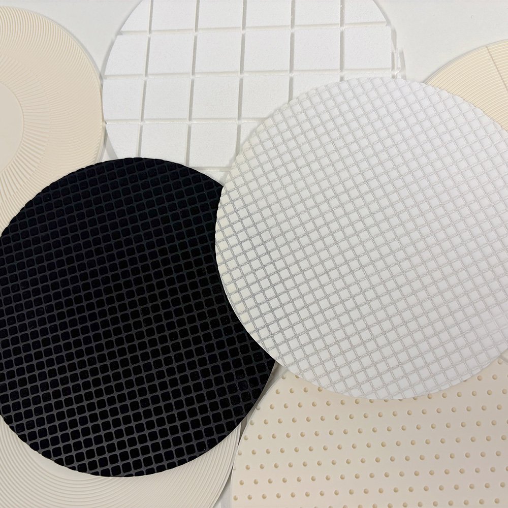
Key Property Profiles — Visual Comparison for Hard PU vs. Soft PU vs. Poreless
8. Material Selection Decision Framework
With the material classes fully characterized, the practical question is: which material is right for a specific CMP step? The following framework provides a systematic selection path based on three primary criteria — target film, node requirement, and defect budget.
Identify the Target Film and Its Hardness
SiO₂, low-k dielectric, Cu, W, barrier nitride, or compound semiconductor (SiC, GaN)? Ultra-hard materials (Mohs >8) require fixed-abrasive or specialty hard-PU pads. Standard IC films (SiO₂, Cu, W) can be addressed with conventional PU systems. The target film hardness narrows the candidate material list immediately.
Define the Primary Process Priority: Planarization vs. Uniformity
If the primary need is step-height reduction (e.g., shallow trench isolation, pre-metal dielectric planarization), hard PU or poreless film is indicated. If the primary need is within-wafer uniformity on a film with low incoming topography (e.g., final Cu overburden clearing, low-k inter-layer), soft PU or a stacked configuration is preferred. These two objectives are in direct tension — the material choice determines which side of the trade-off you land on.
Assess the Defect Budget
At nodes ≤7 nm, or for any CMP step preceding a high-resolution lithography level, the post-CMP scratch and particle defect budget is extremely tight. In this regime, poreless film pads are strongly preferred despite their cost premium. For mature nodes or non-critical process steps, the defect density of standard filled-PU pads is typically acceptable and the cost advantage of conventional pads is decisive.
Factor in Economic Constraints
Total cost of ownership (TCO) — not just pad unit price — drives the economic decision. A poreless pad at 3× the price of a conventional pad may be TCO-positive if it eliminates 5 wafer rework events per quarter at a cost of several thousand dollars each. Conversely, for a mature-node oxide CMP step where defect yields are already excellent, switching to a poreless pad at 3× the price delivers no incremental value. For a detailed procurement analysis, see: CMP Polishing Pad Price Factors and Buying Guide.
9. Polyurethane Chemistry Deep Dive: What Process Engineers Need to Know
Because polyurethane dominates the CMP pad market, a deeper understanding of its chemistry is valuable for anyone specifying, qualifying, or troubleshooting CMP pads. The three most process-relevant aspects of PU chemistry are hydrolytic stability, thermal degradation behavior, and slurry-chemical compatibility.
Hydrolytic Stability: Polyol Backbone Matters
Polyurethane pads used in alkaline slurry environments (pH 10–11, common in oxide CMP with ceria slurries) are subject to hydrolytic degradation of the urethane linkages over time. The rate of hydrolysis depends strongly on the polyol backbone:
| Polyol Type | Hydrolytic Stability | Application typique | Trade-off |
|---|---|---|---|
| Polyether polyol | Moderate (ether linkage vulnerable to oxidation) | General oxide CMP, legacy nodes | Low cost; moderate chemical resistance |
| Polyester polyol | Poor (ester hydrolysis at high pH) | Dry or near-neutral pH applications only | Excellent initial hardness; degrades in alkaline slurry |
| Polycarbonate polyol | Excellent (carbonate linkage highly resistant) | Advanced node oxide, W, high-pH slurry applications | Higher raw material cost; most stable option |
| Polysiloxane-modified PU | Excellent (Si-O backbone) | Very aggressive oxidizer slurries (KMnO₄, high-conc. H₂O₂) | Specialty material; limited supplier base |
Thermal Degradation: The Tg Ceiling
As pad surface temperature rises during polishing — driven by frictional heat generation — the polymer approaches its glass transition temperature (Tg). Above Tg, the polymer transitions from a glassy, elastic solid to a rubbery, viscous material. For CMP pads, operating near Tg causes rapid glazing, asperity collapse, and MRR drift. Selection of a pad with Tg well above the expected process temperature is essential.
Chemical Compatibility: Beyond pH
Slurry-pad chemical compatibility extends beyond pH resistance. Three specific chemical classes require verification during pad qualification:
- Strong oxidizers (KMnO₄, H₂O₂ >5%, O₃): Can oxidize PU chain segments, accelerating surface degradation and increasing debris generation. Polycarbonate-backbone PU and polysiloxane-modified PU offer the best resistance.
- Organic additives (BTA, glycine, citric acid): Most PU formulations show excellent resistance to these low-concentration organic complexing agents. However, high-concentration BTA (used in some Cu CMP slurries) can plasticize certain polyether PU formulations, reducing hardness during polishing.
- Surfactants: Used in low-k CMP slurries to reduce surface tension, surfactants can swell soft PU foams over extended polishing campaigns, gradually increasing compressibility and shifting the process window. Verify with 24-hour immersion tests at process concentration and temperature.