Waxless Polishing Templates vs. Wax Mounting: Cost, Quality & Process Comparison
Two fundamentally different approaches to holding a wafer during single-side polishing. One has been the industry standard for decades. The other has largely replaced it — and for good reason.
The Origins of Wax Mounting in Wafer Polishing
Wax mounting has been part of semiconductor wafer polishing since the earliest commercial silicon wafer production in the 1960s. The logic was straightforward: to polish one face of a wafer flat, you need to fix the other face to a rigid, flat reference surface. Wax provided a simple, inexpensive adhesive that could bond the wafer backside to a polishing block at moderate temperature, hold it rigidly during polishing, and release it with a controlled thermal or solvent debonding step.
For decades, wax mounting worked well enough. The semiconductor industry’s wafer specifications were less demanding, process control methods were less sophisticated, and the hidden costs of the wax cycle — the dedicated waxing equipment, the solvent dewax station, the cleaning steps, the thermal stress on the wafer — were simply absorbed as the cost of doing business. Nobody questioned them because there was no alternative.
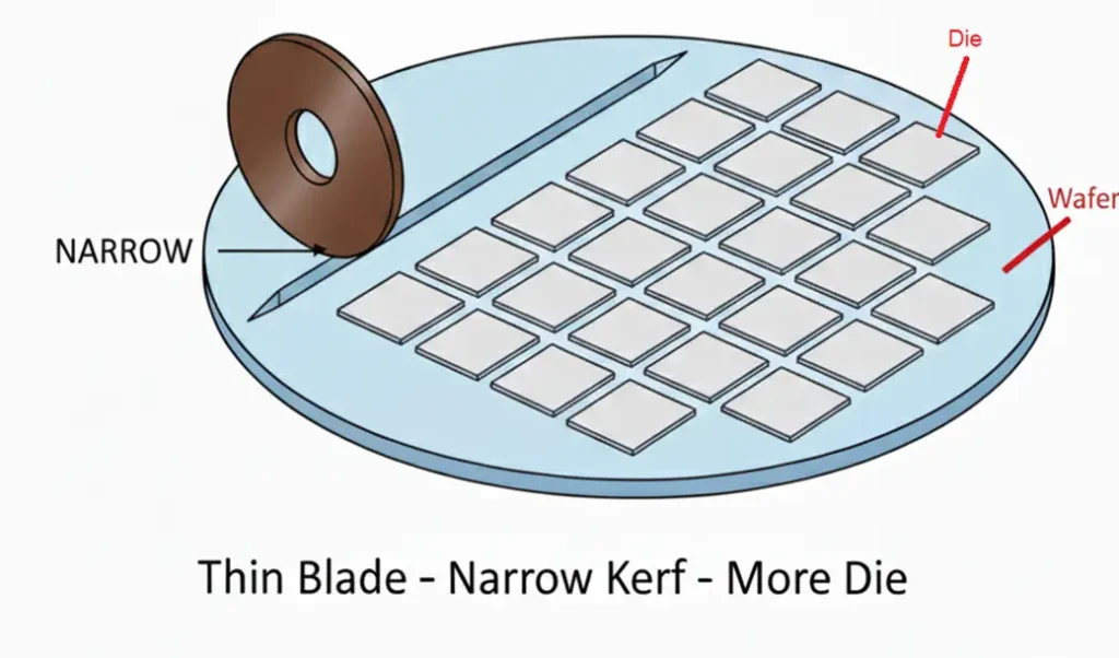
The alternative arrived in the form of the waxless polishing template: a fixture that uses capillary adhesion rather than chemical bonding to hold the wafer, making the entire wax cycle unnecessary. Understanding how polishing templates work at a fundamental level makes clear why capillary retention is both mechanically sound and process-superior to wax bonding for the vast majority of semiconductor polishing applications.
How Wax Mounting Works: The Traditional Process
In a traditional wax mount polishing operation, wafer fixturing is a multi-step thermal process that occurs both before and after polishing. The wax used is typically a hard paraffin or modified rosin compound with a softening point in the 60–90°C range, chosen to be rigid at room temperature polishing conditions while flowing and releasing at elevated temperature.
The Wax Mount Sequence
Before polishing begins, the polishing block (a flat ceramic or metal reference surface) is heated to above the wax softening point, typically 70–85°C on a temperature-controlled hot plate. A measured amount of wax is applied to the block surface and allowed to melt into a uniform film. The wafer is placed backside-down onto the molten wax and pressed with a calibrated weight or pneumatic fixture to ensure uniform contact and defined wax layer thickness. The assembly is then cooled to room temperature, during which the wax solidifies and bonds the wafer to the block. The bonded assembly is loaded into the polishing machine and the front face is polished in the normal manner.
After polishing, the block-and-wafer assembly is re-heated to above the wax softening point. The wafer is gently slid or lifted from the block as the wax melts. The wafer is then transferred to a solvent dewax bath — typically acetone, IPA, or a proprietary dewax solvent — where residual wax is dissolved from the wafer backside by agitation and heating. A DI water rinse and spin-dry complete the post-polishing handling sequence before the wafer can enter any subsequent process step.
The Problems Wax Mounting Creates
Wax mounting works. But it works while creating a cascade of secondary problems that compound across the process flow, the quality record, and the cost structure of a polishing operation. These problems were tolerable when there was no alternative. They are not tolerable when a better solution exists.
1. Systematic TTV Contribution from Wax Layer Non-Uniformity
As noted above, wax layer thickness variation maps directly into finished wafer TTV. This is a fundamental, irreducible limitation of the wax mount approach — no amount of process optimization fully eliminates wax layer thickness variation, because it is introduced by a manual or semi-manual application step that has inherent variability. For advanced silicon prime wafers with TTV specifications of 1.0 µm or tighter, the wax layer non-uniformity alone can consume the entire TTV budget.
2. Thermal Stress and Wafer Breakage Risk
Every wax mount cycle exposes the wafer to two thermal excursions: heating for bonding (70–85°C) and heating for debonding (70–85°C again). Silicon has a coefficient of thermal expansion (CTE) of approximately 2.6 × 10⁻⁶/°C. A 300 mm silicon wafer at 80°C expands by approximately 62 µm in diameter relative to room temperature. This thermal expansion, constrained by the wax bond, creates compressive stress in the wafer plane during bonding and tensile stress during cooling. For standard-thickness silicon wafers (775 µm at 300 mm), this stress is well within the fracture limit. For thin wafers below 300 µm, it is a documented breakage risk — one that waxless processing eliminates entirely.
3. Wax Contamination in Downstream Process Steps
Organic wax compounds are persistent contaminants in a semiconductor fab environment. Incomplete dewax cleaning leaves wax residues on the wafer backside that outgas in diffusion furnaces, create adhesion failures in photoresist coat, and introduce organic contamination into ion implant chambers. Even with a fully optimized dewax process, trace wax contamination at the parts-per-billion level on the wafer backside is difficult to eliminate. This is a quality risk that does not exist with waxless processing.
4. Equipment, Chemical, and Labor Cost
A complete wax mount infrastructure requires: a temperature-controlled wax application station, a bonding weight or pneumatic press, a dewax solvent bath with heating and agitation, a solvent recovery or disposal system (wax solvents are typically flammable organics requiring hazmat handling), DI water rinse stations, and dedicated operator time for the mount and demount steps. This infrastructure has both capital and operating cost that is entirely absent from a waxless polishing operation.
5. Throughput Penalty
The wax mount cycle — heat, bond, cool, polish, heat, debond, dewax, rinse, dry — adds 30–60 minutes to the total process time per wafer lot compared to waxless processing, where the template is simply wetted and loaded. At production scale, this throughput penalty translates directly into polisher utilization loss and higher effective cost per polished wafer.
How Waxless Polishing Templates Work
A waxless polishing template solves the wafer fixturing problem through an entirely different physical mechanism: capillary adhesion. The porous backing pad bonded to the template’s rigid carrier plate has a surface structure that, when wetted with deionized water, creates a continuous water film between the pad surface and the smooth wafer backside. Surface tension in this water film generates an adhesive force — the same force that makes two wet glass slides stick together — that is strong enough to hold the wafer firmly against the pad throughout the polishing cycle.
The loading process requires wetting the backing pad with a small volume of DI water (typically applied by spray or pipette), placing the wafer backside-down onto the wetted pad, and pressing gently by hand for 2–3 seconds to establish full contact. The wafer adheres immediately. No heating, no wax, no cure time. The template-and-wafer assembly is loaded into the carrier head and polishing proceeds normally.
After polishing, the wafer is released by one of two methods: either the backing pad is allowed to partially dry (which reduces capillary force below the gravitational force on the wafer), or a gentle mechanical release — a slight edge lift with a plastic spatula — is applied. The release is clean, at room temperature, with no chemical or thermal processing required. The wafer is rinsed and the template is ready for the next cycle after re-wetting.
Side-by-Side Process Flow Comparison
The most concrete way to appreciate the waxless template advantage is to lay the two process flows side by side. The steps struck through in red below represent process steps that are completely eliminated when transitioning from wax mounting to waxless templates.
Wax mounting: 10 process steps (including 3 thermal events and 1 hazardous solvent step). Waxless template: 5 process steps (no thermal events, no solvents). 5 steps eliminated — a 50% reduction in polishing process cycle complexity.
TTV & Surface Quality: What the Process Data Shows
The TTV comparison between wax mounting and waxless template processing is one of the most-studied topics in silicon wafer polishing process engineering, and the findings are consistent across production data from multiple fab environments and wafer diameter nodes.
Wax Layer Non-Uniformity as a TTV Floor
In wax mount polishing, the total measured TTV on the finished wafer is the sum of two contributions: the TTV generated by the polishing process itself (machine-related, pad-related, and template-related sources), and the TTV contributed by wax layer thickness non-uniformity. The second term is a systematic baseline that can be minimized through wax application process control but cannot be eliminated. Depending on the wax application method — hand spread, automated dispense, or spin coat — this wax-contribution term is typically in the range of 0.3–1.5 µm for 200 mm wafers and 0.5–2.0 µm for 300 mm wafers.
In waxless template processing, the wax layer non-uniformity term is zero by definition. The total measured TTV is purely a function of the template geometry and the polishing process. This is not a marginal improvement — for any application with a TTV specification below 2.0 µm, the wax layer contribution is a non-negligible fraction of the total budget.
Back-Surface Quality
Wax mount polishing consistently produces higher back-surface particle counts than waxless processing, for two reasons. First, wax residues left after incomplete dewax cleaning introduce organic particles. Second, the thermal cycle during wax application and removal can stress-relieve pre-existing micro-cracks in the wafer backside, releasing silicon particles. Waxless processing eliminates both sources, producing cleaner wafer backsides that pass tighter incoming inspection criteria at device fabrication customers.
| Quality Metric | Wax Mounting | Waxless Template | Advantage |
|---|---|---|---|
| TTV (300 mm Si prime) | 1.5–3.5 µm typical | 0.8–2.0 µm typical | Waxless |
| Wax layer contribution to TTV | 0.5–2.0 µm (irreducible) | 0 µm | Waxless |
| Lot-to-lot TTV repeatability | Moderate — limited by wax application variation | High — template geometry is stable | Waxless |
| Back-surface particle count | Higher — wax residue risk | Lower — no organic residue | Waxless |
| Edge profile control | Limited by wax block geometry | Engineerable via template/EER design | Waxless |
| Rugosité de la surface (Ra) | Equivalent | Equivalent | Tie |
Contamination & Cleanroom Impact
Wax mounting introduces two categories of contamination risk that waxless processing eliminates: organic chemical contamination from wax and dewax solvents, and particulate contamination from wax residues and solvent handling.
Organic Contamination
Wax compounds are organic materials — typically paraffin, carnauba, or modified rosin formulations. In a semiconductor cleanroom, organic materials are a contamination class that must be carefully controlled, because they can adsorb onto silicon surfaces and create adhesion failures in oxide growth, resist coat, and metal deposition steps downstream. Trace wax contamination surviving the dewax cleaning step is measured in parts-per-billion on the wafer surface by TOC (total organic carbon) analysis. Achieving TOC levels below 50 ppb C on wax-processed wafers requires multiple solvent rinse steps with tightly controlled bath lifetime management.
Waxless processing eliminates the organic contamination source entirely. There is no wax on the wafer at any point — the only fluid in contact with the wafer backside is DI water, which has no organic contribution. This simplifies cleanroom chemical management, reduces the number of chemical baths requiring maintenance and titration, and eliminates one organic contamination monitoring point from the wafer quality inspection flow.
Solvent Handling in Cleanroom Environments
Acetone and IPA — the most common wax dewax solvents — are Class IB and Class II flammable liquids respectively under NFPA classification. Their use in a cleanroom requires dedicated flammable storage cabinets, explosion-proof exhaust ventilation, chemical spill containment, and hazardous waste disposal protocols. These requirements add facility infrastructure cost and regulatory compliance burden that disappears when waxless processing eliminates the dewax step. For a facility running exclusively waxless templates, the entire wax and solvent chemical management program can be decommissioned.
Maintaining cleanroom integrity is also important at the template level — our article on contamination control in polishing templates covers both supplier-side assembly practices and in-fab handling protocols.
Thin Wafer & Fragile Substrate Handling
The thermal stress argument against wax mounting becomes decisive when the substrate is thin, brittle, or thermally sensitive. Three substrate categories are particularly relevant.
Ultra-Thin Silicon Wafers (< 300 µm)
Back-end-of-line (BEOL) thinning processes and power device applications regularly produce silicon wafers with final thicknesses in the 100–300 µm range. At these thicknesses, the wafer’s mechanical rigidity is significantly reduced, and the thermal gradient created by placing a room-temperature wafer onto an 80°C wax block — or by lifting a hot wafer off the debonding station — creates bending moments that exceed the fracture toughness of the wafer. Wax mount breakage rates for 200 mm silicon below 200 µm are documented in the 0.5–2.0% range depending on process conditions. Waxless processing at room temperature reduces this breakage mode to essentially zero.
Compound Semiconductor Substrates (GaAs, InP)
Gallium arsenide and indium phosphide have fracture toughness approximately 25% that of silicon, combined with a CTE that differs significantly from most wax block materials. The CTE mismatch between GaAs (5.8 × 10⁻⁶/°C) and a ceramic polishing block (4–7 × 10⁻⁶/°C, depending on composition) creates differential thermal stress during the wax cycle that is a primary driver of GaAs wafer cracking in transit between the bonding station and the polishing machine. Waxless templates, with their room-temperature load and release, are the standard choice for GaAs and InP polishing. The engineering requirements for compound semiconductor templates are covered in our article on GaAs, InP, and sapphire polishing templates.
Device Wafers with Patterned Front Faces
Back-side polishing of wafers with completed or partially completed device layers on the front face requires that the front surface be protected during polishing. In wax mount processes, protecting a patterned front face from wax contamination requires an additional protective layer deposition and removal step. Waxless templates contact only the wafer backside and require no front-face protection, simplifying the process flow for back-side polishing applications.
Total Cost of Ownership: A Structured Analysis
The unit cost of a waxless polishing template is higher than the unit cost of the wax materials it replaces for a single polishing cycle. This is the most commonly cited argument against waxless processing — and it is also the most misleading, because it compares one consumable line item in isolation against the full system cost of the wax mount process.
A proper total cost of ownership (TCO) comparison must include all cost elements that differ between the two approaches across a defined production period. The analysis below is structured for a representative 300 mm silicon wafer SSP production line polishing 5,000 wafers per month.
On a fully-loaded cost basis including labor, chemical management, equipment amortization, and breakage, waxless template processing is consistently $0.50–2.00 per wafer cheaper than wax mounting for 300 mm silicon SSP — despite a higher template unit cost. At 5,000 wafers per month, this represents a $2,500–10,000 monthly cost reduction, before accounting for the yield improvement from lower TTV and cleaner wafer backsides.
Substrate Compatibility Overview
Waxless template technology is applicable to the full range of semiconductor substrates. The following summary covers the most common substrate types and their waxless compatibility status. Detailed substrate-specific engineering is covered in the linked articles.
Silicon (Si) — All Diameters
PreferredStandard FR-4 or G-10 templates with alkaline-slurry-compatible backing pads. Industry-standard choice for all Si SSP production at 100–300 mm.
SiC — 100 mm, 150 mm
CompatibleRequires CXT-grade chemically resistant templates. Waxless approach preferred due to long SiC polishing cycle times (thermal stress in wax would be severe). See SiC template guide.
GaAs / InP
Strongly PreferredWaxless is strongly preferred over wax for III-V substrates due to CTE mismatch breakage risk. Soft backing pad compound required for fracture-sensitive materials.
Saphir
CompatibleG-10 or CXT templates with medium-hard backing pads. Waxless eliminates the thermal stress risk inherent in wax mounting of sapphire’s high-CTE crystal structure.
Glass Substrates
CompatibleG-10 templates for standard glass polishing. Thin glass (<300 µm) benefits particularly from waxless room-temperature processing. See glass substrate guide.
Ultra-Thin Si (<200 µm)
Strongly PreferredWaxless is the only low-risk option for sub-200 µm silicon. Thermal cycle breakage rates of 0.5–2% in wax mount are eliminated entirely with waxless processing.
When Wax Mounting Is Still Used
Despite the comprehensive advantages of waxless polishing templates, wax mounting has not completely disappeared from the semiconductor industry. There are specific application contexts where it remains in use, though even in these cases the trend is toward waxless transition.
Legacy Production Lines with Established Wax Processes
Some fabs running older, established product lines on legacy polishing equipment have not transitioned to waxless templates because the wax process is qualified, the TTV specification is met, and the business case for re-qualification is not compelling for a mature product with limited remaining lifetime. This is a valid economic decision, not a technical endorsement of wax mounting. As these product lines reach end-of-life and equipment is replaced or re-qualified, the transition to waxless is universally chosen for new qualifications.
Certain Optical and Precision Optics Applications
Outside the semiconductor wafer market, wax mounting remains standard in precision optics polishing — lenses, prisms, and optical flats — where the substrate geometries are highly irregular and the capillary retention mechanism of waxless templates cannot provide the positional accuracy required. This application is distinct from semiconductor wafer polishing and does not apply to the substrate types covered in this article.
Very High Material Removal Rate Processes
For processes requiring extremely high polishing pressures (above 10 psi) and long polishing times — such as initial stock removal on as-cut SiC ingot slices — wax bonding to a rigid block can provide higher retention force than capillary adhesion on a waxless template. However, this represents a very small subset of SiC processing, limited to the first coarse lapping step; CMP and final polish steps on SiC use waxless CXT-grade templates. For standard semiconductor wafer polishing pressures, waxless template retention is always sufficient.