
Oxide CMP Slurry Recycling & Sustainability: A Fab Implementation Guide
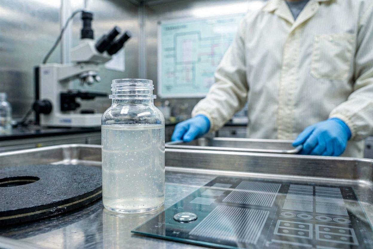
📅 July 2026·⏱ 15 min read·✍️ JEEZ Technical Team Oxide CMP slurry represents one of the largest chemical waste streams in semiconductor manufacturing by volume. At a production 300 mm ...


